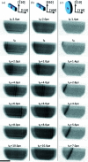
Brittle fracture studied by ultra-high-speed synchrotron X-ray diffraction imaging
- PMID: 35974730
- PMCID: PMC9348878
- DOI: 10.1107/S1600576722006537
Brittle fracture studied by ultra-high-speed synchrotron X-ray diffraction imaging
Abstract
In situ investigations of cracks propagating at up to 2.5 km s-1 along an (001) plane of a silicon single crystal are reported, using X-ray diffraction megahertz imaging with intense and time-structured synchrotron radiation. The studied system is based on the Smart Cut process, where a buried layer in a material (typically Si) is weakened by microcracks and then used to drive a macroscopic crack (10-1 m) in a plane parallel to the surface with minimal deviation (10-9 m). A direct confirmation that the shape of the crack front is not affected by the distribution of the microcracks is provided. Instantaneous crack velocities over the centimetre-wide field of view were measured and showed an effect of local heating by the X-ray beam. The post-crack movements of the separated wafer parts could also be observed and explained using pneumatics and elasticity. A comprehensive view of controlled fracture propagation in a crystalline material is provided, paving the way for the in situ measurement of ultra-fast strain field propagation.
Keywords: X-ray diffraction; crack-front shape; ion implantation.
© Antoine Petit et al. 2022.
Figures


References
-
- Agarwal, A., Haynes, T. E., Venezia, V. C., Holland, O. W. & Eaglesham, D. J. (1998). Appl. Phys. Lett. 72, 1086–1088.
-
- Aspar, B., Bruel, M., Moriceau, H., Maleville, C., Poumeyrol, T., Papon, A. M., Claverie, A., Benassayag, G., Auberton-Hervé, A. J. & Barge, T. (1997). Microelectron. Eng. 36, 233–240.
-
- Atrash, F., Meshi, I., Krokhmal, A., Ryan, P., Wormington, M. & Sherman, D. (2017). Mater. Sci. Semicond. Process. 63, 40–44.
-
- Bruel, M. (1995). Electron. Lett. 31, 1201–1202.
-
- Claverie, A., Daix, N., Okba, F. & Cherkashin, N. (2018). 22nd International Conference on Ion Implantation Technology (IIT), 16–21 September 2018, Würzburg, Germany, pp. 128–131. New York: IEEE.
LinkOut - more resources
Full Text Sources
