. 2022 Aug;608(7923):504-512.
doi: 10.1038/s41586-022-04992-8. Epub 2022 Aug 17.

A compute-in-memory chip based on resistive random-access memory

Affiliations

A compute-in-memory chip based on resistive random-access memory

Weier Wan et al. Nature. 2022 Aug.

Abstract

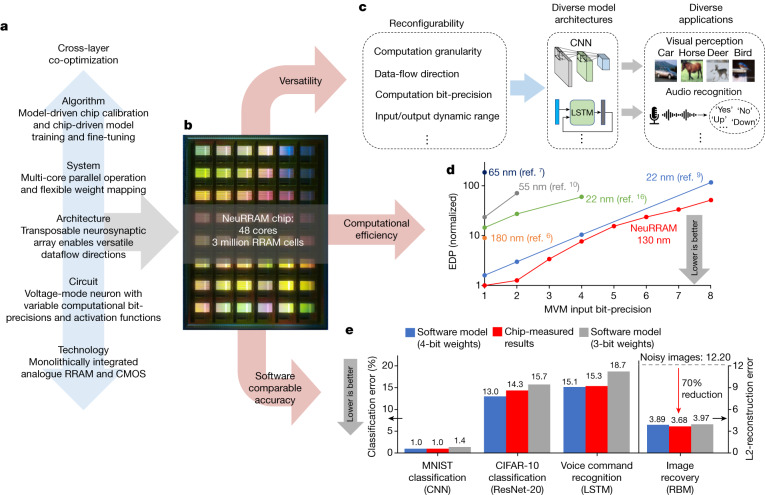
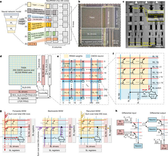
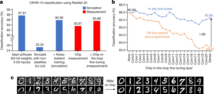
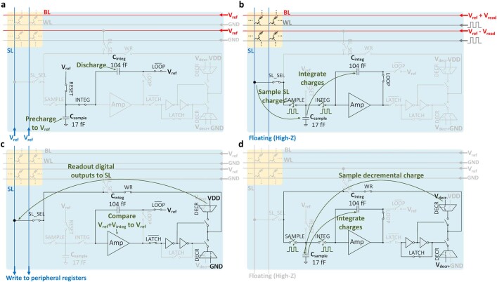
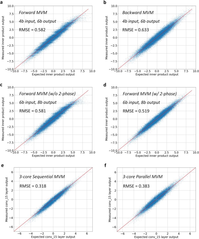
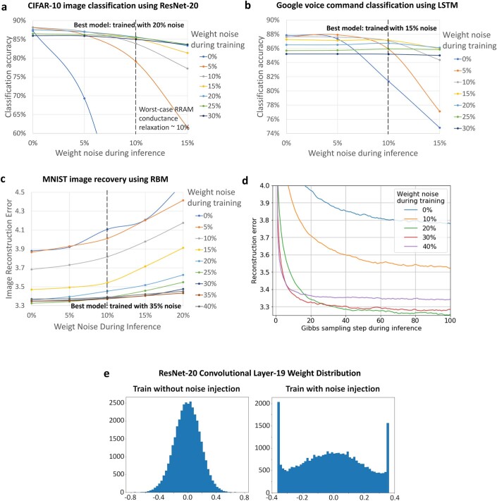
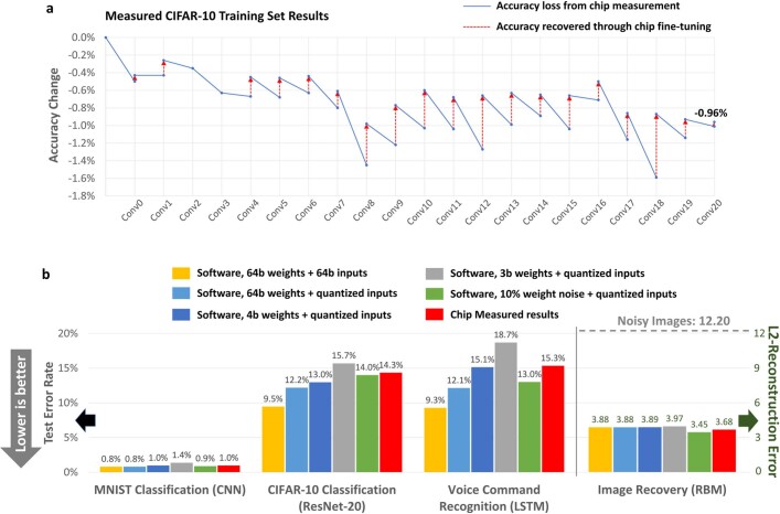
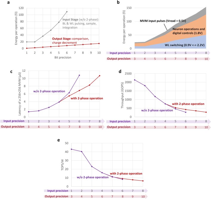
Realizing increasingly complex artificial intelligence (AI) functionalities directly on edge devices calls for unprecedented energy efficiency of edge hardware. Compute-in-memory (CIM) based on resistive random-access memory (RRAM)1 promises to meet such demand by storing AI model weights in dense, analogue and non-volatile RRAM devices, and by performing AI computation directly within RRAM, thus eliminating power-hungry data movement between separate compute and memory2-5. Although recent studies have demonstrated in-memory matrix-vector multiplication on fully integrated RRAM-CIM hardware6-17, it remains a goal for a RRAM-CIM chip to simultaneously deliver high energy efficiency, versatility to support diverse models and software-comparable accuracy. Although efficiency, versatility and accuracy are all indispensable for broad adoption of the technology, the inter-related trade-offs among them cannot be addressed by isolated improvements on any single abstraction level of the design. Here, by co-optimizing across all hierarchies of the design from algorithms and architecture to circuits and devices, we present NeuRRAM-a RRAM-based CIM chip that simultaneously delivers versatility in reconfiguring CIM cores for diverse model architectures, energy efficiency that is two-times better than previous state-of-the-art RRAM-CIM chips across various computational bit-precisions, and inference accuracy comparable to software models quantized to four-bit weights across various AI tasks, including accuracy of 99.0 percent on MNIST18 and 85.7 percent on CIFAR-1019 image classification, 84.7-percent accuracy on Google speech command recognition20, and a 70-percent reduction in image-reconstruction error on a Bayesian image-recovery task.


Conflict of interest statement

The authors declare no competing interests.

Figures

Fig. 1
Fig. 1. Design methodology and main contributions of the NeuRRAM chip.
a, Cross-layer co-optimizations across the full stack of the design enable NeuRRAM to simultaneously deliver high versatility, computational efficiency and software-comparable inference accuracy. b, Micrograph of the NeuRRAM chip. c, Reconfigurability in various aspects of the design enables NeuRRAM to implement diverse AI models for a wide variety of applications. d, Comparison of EDP, a commonly used energy-efficiency and performance metric among recent RRAM-based CIM hardware. e, Fully hardware-measured inference accuracy on NeuRRAM is comparable to software models quantized to 4-bit weights across various AI benchmarks.
Fig. 2
Fig. 2. Reconfigurable architecture of the NeuRRAM chip.
a, Multi-core architecture of the NeuRRAM chip, and various ways, labelled (1) to (6), to map neural-network layers onto CIM cores. b, Zoomed-in chip micrograph on a single CIM core. c, A cross-sectional transmission electron microscopy image showing the layer stack of the monolithically integrated RRAM and CMOS. d, Block diagram of a CIM core. A core consists of a TNSA, drivers for BLs, WLs, and SLs, registers that store MVM inputs and outputs, a LFSR pseudo-random number generator (PRNG), and a controller. During the MVM input stage, the drivers convert register inputs (REG) and PRNG inputs (PRN) to analogue voltages and send them to TNSA; during the MVM output stage, the drivers pass digital outputs from neurons back to registers through REG. e, The architecture of a TNSA consists of 16 × 16 corelets with interleaving RRAM weights and CMOS neurons. Each neuron integrates inputs from 256 RRAMs connecting to the same horizontal BL or vertical SL. f, Each corelet contains 16 × 16 RRAMs and 1 neuron. The neuron connects to 1 of the 16 BLs and 1 of the 16 SLs that pass through the corelet, and can use a BL and a SL for both its input and output. g, The TNSA can be dynamically configured for MVM in forwards, backwards or recurrent directions. h, Differential input and differential output schemes used to implement real-valued weights during forwards and backwards MVMs. Weights are encoded as the differential conductance between two RRAM cells on adjacent rows (G+ and G-).
Fig. 3
Fig. 3. Voltage-mode MVM with multi-bit inputs and outputs.
a, Conventional current-mode-sensing scheme needs to activate a small fraction of total N rows each cycle to limit total current ISL and time-multiplex ADCs across multiple columns to amortize ADC area, thus limiting its computational parallelism. b, Voltage-mode sensing employed by NeuRRAM can activate all the rows and all the columns in a single cycle, enabling higher parallelism. c, MVM output distribution from a CNN layer and from an LSTM layer (weights normalized to the same range). Voltage-mode sensing intrinsically normalizes wide variation in output dynamic range. d, Schematic of the voltage-mode neuron circuit, where BLsel, SLsel, Sample, Integ, Reset, Latch, Decr, and WR are digital signals controlling state of the switches. e, Sample waveforms to perform MVM and 4-bit signed inputs digital-to-analogue conversion. WLs are pulsed once per magnitude-bit; sampling and integration are performed 2n−1 times for the nth LSB. f, Two-phase MVM: for input precision greater than 4 bits, inputs are divided into a MSB segment and a LSB segment. MVMs and ADCs are performed separately for each segment, followed by a shift-and-add to obtain final outputs. g, Sample waveforms to perform 5-bit signed outputs analogue-to-digital conversion. The sign-bit is first generated by a comparison operation. The magnitude-bits are generated through a binary search process realized by adding/subtracting charge on Cinteg. From MSB to LSB, added/subtracted charge is halved every bit. h, Chip-measured 64 × 64 MVM outputs versus ideal outputs under 4-bit input and 6-bit output.
Fig. 4
Fig. 4. Hardware-algorithm co-optimization techniques to improve NeuRRAM inference accuracy.
a, Various device and circuit non-idealities (labelled (1) to (7)) of in-memory MVM. b, Model-driven chip calibration technique to search for optimal chip operating conditions and record offsets for subsequent cancellation. c, Noise-resilient neural-network training technique to train the model with noise injection. The noise distribution is obtained from hardware characterization. The trained weights are programmed to the continuous analogue conductance of RRAMs without quantization as shown by the continuous diagonal band at the bottom. d, Chip-in-the-loop progressive fine-tuning technique: weights are progressively mapped onto the chip one layer at a time. The hardware-measured outputs from layer n are used as inputs to fine-tune the remaining layers n + 1 to N.
Fig. 5
Fig. 5. Measured results showing the efficacy of the hardware-algorithm co-optimization techniques.
a, Simulated (blue) and measured (red) CIFAR-10 test-set classification accuracies. b, CIFAR-10 classification accuracy at various time steps of chip-in-the-loop fine-tuning. From left to right, each data point represents a new layer (Conv0 to Dense) programmed onto the chip. The accuracy at a layer is evaluated by using the hardware-measured outputs from that layer as inputs to the remaining layers that are simulated in software. Two curves compare the test-set inference accuracy with and without applying fine-tuning during training. c, RBM-based image recovery on noisy images (top) and partially occluded images measured on NeuRRAM (bottom).
Extended Data Fig. 1
Extended Data Fig. 1. Peripheral driver circuits for TNSA and chip operating modes.
a, driver circuits’ configuration under the weight-programming mode. b, under the neuron-testing mode. c, under the MVM mode. d, circuit diagram of the two counter-propagating LFSR chains XORed to generate pseudo-random sequences for probabilistic sampling.
Extended Data Fig. 2
Extended Data Fig. 2. Various MVM dataflow directions and their CIM implementations.
Left, various MVM dataflow directions commonly seen in different AI models. Middle, conventional CIM implementation of various dataflow directions. Conventional designs typically locate all peripheral circuits such as ADCs outside of RRAM array. The resulting implementations of bidirectional and recurrent MVMs incur overheads in area, latency, and energy. Right, the Transposable Neurosynaptic Array (TNSA) interleaves RRAM weights and CMOS neurons across the array and supports diverse MVM directions with minimal overhead.
Extended Data Fig. 3
Extended Data Fig. 3. Iterative write–verify RRAM programming.
a, Flowchart of the incremental-pulse write–verify technique to program RRAMs into target analogue conductance range. b, An example sequence of the write–verify programming. c, RRAM conductance distribution measured during and after the write–verify programming. Each blue dot represents one RRAM cell measured during write–verify. The grey shades show that the RRAM conductance relaxation cause the distribution to spread out from the target values. The darker shade shows that the iterative programming helps narrow the distribution. d, Standard deviation of conductance change measured at different initial conductance states and different time duration after the initial programming. The initial conductance relaxation happens at a faster rate than longer term retention degradation. e, Standard deviation of conductance relaxation decreases with increasing iterative programming cycles. f, Distribution of the number of SET/RESET pulses needed to reach conductance acceptance range.
Extended Data Fig. 4
Extended Data Fig. 4. 4 basic neuron operations that enable MVM with multi-bit inputs and outputs.
a, Initialization, precharge sampling capacitor Csample and output wires (SLs), and discharge integration capacitor Cinteg. b, Sampling and integration, sample SL voltage onto Csample, followed by integrating the charge onto Cinteg. c, Comparison and readout. The amplifier is turned into comparator mode to determine the polarity of the integrated voltage. Comparator outputs are written out of the neuron through the outer feedback loop. d, Charge decrement, charge is added or subtracted on Cinteg through the outer feedback loop, depending on value stored in the latch.
Extended Data Fig. 5
Extended Data Fig. 5. Scatter plots of measured MVMs vs. ideal MVMs.
Results in a-d are generated using the same 64×64 normally distributed random matrix and 1000 uniformed distributed floating-point vectors ϵ [-1, 1]. a, Forward MVM using differential input scheme with inputs quantized to 4-bit and outputs 6-bit. b, Backward MVM using differential output scheme. The higher RMSE is caused by more voltage drop on each SL driver that needs to drive 128 RRAM cells, compared to 64 cells driven by each BL driver during forward MVM. c, MVM root-mean-square error (RMSE) does not reduce when increasing input from 4-bit (a) to 6-bit. This is caused by using a lower input voltage that leads to worse signal-to-noise-ratio. d, 2-phase operation reduces MVM RMSE with 6-bit input by breaking inputs into 2 segments and performing MVMs separately, such that input voltage does not need to be reduced. e–f, Outputs from conv15 layer of ResNet-20. Weights of conv15 are divided to 3 CIM cores. Layer outputs show a higher RMSE when performing MVM in parallel on the 3 cores (f) than sequentially on the 3 cores (e).
Extended Data Fig. 6
Extended Data Fig. 6. Data distribution with and without model-driven chip calibration.
Left, Distribution of inputs to the final fully connected layer of ResNet-20 when the inputs are generated from (top-to-bottom) CIFAR-10 test-set data, training-set data, and random uniform data. Right, Distribution of outputs from the final fully connected layer of ResNet-20. The test-set and training-set have similar distributions while random uniform data produces a markedly different output distribution. To ensure that the MVM output voltage dynamic range during testing is calibrated to occupy the full ADC input swing, the calibration data should come from training-set data that closely resembles the test-set data.
Extended Data Fig. 7
Extended Data Fig. 7. Noise-resilient training of CNNs, LSTMs and RBMs.
a, Change in CIFAR-10 test-set classification accuracy under different weight noise levels during inference. Noise is represented as fraction of the maximum absolute value of weights. Different curves represent models trained at different levels of noise injection. b, Change in voice command recognition accuracy with weight noise levels. c, Change in MNIST image-reconstruction error with weight noise levels. d, Decreasing of image-reconstruction error with Gibbs sampling steps during RBM inference. e, Differences in weight distributions when trained without and with noise injection.
Extended Data Fig. 8
Extended Data Fig. 8. Measured chip inference performance.
a, CIFAR-10 training-set accuracy loss due to hardware non-idealities, and accuracy recovery at each step of the chip-in-the-loop progressive fine-tuning. From left to right, each data point represents a new layer programmed onto the chip. The blue solid lines represent the accuracy loss measured when performing inference of that layer on-chip. The red dotted lines represent the measured recovery in accuracy by fine-tuning subsequent layers. b, Ablation study showing the impacts of input, activation, and weight quantizations, and weight noise injection on inference errors.
Extended Data Fig. 9
Extended Data Fig. 9. Implementation of various AI models.
a, Architecture of ResNet-20 for CIFAR-10 classification. b, The batch normalization parameters are merged into convolutional weights and biases before mapping on-chip. c, Illustration of the process to map 4-dimensional weights of a convolutional layer to NeuRRAM CIM cores. d, Architecture of the LSTM model used for Google speech command recognition. The model contains 4 parallel LSTM cells and makes predictions based on the sum of outputs from the 4 cells. e, Architecture of the RBM model used for MNIST image recovery. During inference, MVMs and Gibbs sampling are performed back and-forth between visible and hidden neurons. f, Process to map RBM on NeuRRAM CIM cores. Adjacent pixels are assigned to different cores to equalize the MVM output dynamic range at different cores.
Extended Data Fig. 10
Extended Data Fig. 10. Chip-measured image recovery using RBM.
Top: Recovery of MNIST test-set images with randomly selected 20% of pixels flipped to complementary intensity. Bottom: Recovery of MNIST test-set images with bottom 1/3 of pixels occluded.
Extended Data Fig. 11
Extended Data Fig. 11. NeuRRAM test system and chip micrographs at various scales.
a, A NeuRRAM chip wire-bonded to a package. b, Measurement board that connects a packaged NeuRRAM chip (left) to a field-programmable gate array (FPGA, right). The board houses all the components necessary to power, operate and measure the chip. No external lab equipment is needed for the chip operations. c, Micrograph of a 48-core NeuRRAM chip. d, Zoomed-in micrograph of a single CIM core. e, Zoomed-in micrograph of 2×2 corelets within the TNSA. One neuron circuit occupies 1270 μm2, which is >100× smaller than most ADC designs in 130-nm summarized in an ADC survey. f, Chip area breakdown.
Extended Data Fig. 12
Extended Data Fig. 12. Energy consumption, latency, and throughput measurement results.
a, Measured energy consumption per operation during the MVM input stage (without 2-phase operation) and output stage, where one multiply–accumulate (MAC) counts as two operations. b, Energy consumption breakdown at various MVM input and output bit-precisions. Outputs are 2-bit higher than inputs during a MVM to account for additional precision requirements from partial-sum accumulation. c, Latency for performing one MVM with 256×256 weight matrix. d, Peak computational throughput (in giga-operations per second). e, Throughput-power efficiency (in tera-operations per watt).

References

    1. Wong HSP, et al. Metal-oxide RRAM. Proc. IEEE. 2012;100:1951–1970. doi: 10.1109/JPROC.2012.2190369. - DOI
    1. Prezioso M, et al. Training and operation of an integrated neuromorphic network based on metal-oxide memristors. Nature. 2015;521:61–64. doi: 10.1038/nature14441. - DOI - PubMed
    1. Ambrogio S, et al. Equivalent-accuracy accelerated neural-network training using analogue memory. Nature. 2018;558:60–67. doi: 10.1038/s41586-018-0180-5. - DOI - PubMed
    1. Ielmini D, Wong HSP. In-memory computing with resistive switching devices. Nat. Electron. 2018;1:333–343. doi: 10.1038/s41928-018-0092-2. - DOI
    1. Yao P, et al. Fully hardware-implemented memristor convolutional neural network. Nature. 2020;577:641–646. doi: 10.1038/s41586-020-1942-4. - DOI - PubMed

Publication types