Review
. 2022 Aug 15;13(8):1318.
doi: 10.3390/mi13081318.

Cesium Lead Iodide Perovskites: Optically Active Crystal Phase Stability to Surface Engineering

Affiliations
Review

Cesium Lead Iodide Perovskites: Optically Active Crystal Phase Stability to Surface Engineering

Yixi Wang et al. Micromachines (Basel). .

Abstract

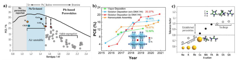
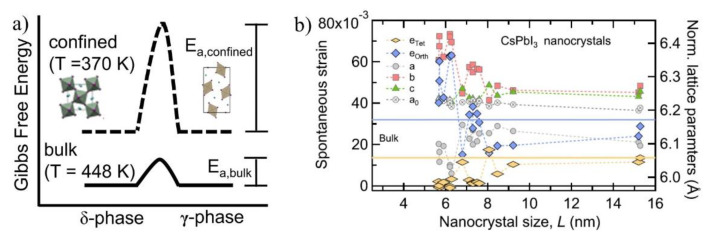
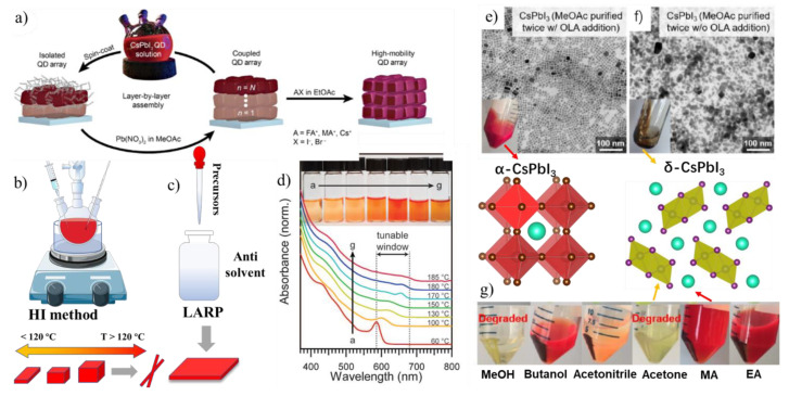
Among perovskites, the research on cesium lead iodides (CsPbI3) has attracted a large research community, owing to their all-inorganic nature and promising solar cell performance. Typically, the CsPbI3 solar cell devices are prepared at various heterojunctions, and working at fluctuating temperatures raises questions on the material stability-related performance of such devices. The fundamental studies reveal that their poor stability is due to a lower side deviation from Goldschmidt's tolerance factor, causing weak chemical interactions within the crystal lattice. In the case of organic-inorganic hybrid perovskites, where their stability is related to the inherent chemical nature of the organic cations, which cannot be manipulated to improve the stability drastically whereas the stability of CsPbI3 is related to surface and lattice engineering. Thus, the challenges posed by CsPbI3 could be overcome by engineering the surface and inside the CsPbI3 crystal lattice. A few solutions have been proposed, including controlled crystal sizes, surface modifications, and lattice engineering. Various research groups have been working on these aspects and had accumulated a rich understanding of these materials. In this review, at first, we survey the fundamental aspects of CsPbI3 polymorphs structure, highlighting the superiority of CsPbI3 over other halide systems, stability, the factors (temperature, polarity, and size influence) leading to their phase transformations, and electronic band structure along with the important property of the defect tolerance nature. Fortunately, the factors stabilizing the most effective phases are achieved through a size reduction and the efficient surface passivation on the delicate CsPbI3 nanocrystal surfaces. In the following section, we have provided the up-to-date surface passivating methods to suppress the non-radiative process for near-unity photoluminescence quantum yield, while maintaining their optically active phases, especially through molecular links (ligands, polymers, zwitterions, polymers) and inorganic halides. We have also provided recent advances to the efficient synthetic protocols for optically active CsPbI3 NC phases to use readily for solar cell applications. The nanocrystal purification techniques are challenging and had a significant effect on the device performances. In part, we summarized the CsPbI3-related solar cell device performances with respect to the device fabrication methods. At the end, we provide a brief outlook on the view of surface and lattice engineering in CsPbI3 NCs for advancing the enhanced stability which is crucial for superior optical and light applications.

Keywords: CsPbI3 NCs; cesium lead iodides; defect-tolerance; hot-injection method; ion exchanges; perovskite crystal structures; perovskite stability; photoluminescence; solar cell; surface engineering.


Conflict of interest statement

The authors declare no conflict to interest.

Figures

Figure 1
Figure 1
(a) Comparison of PCE among different materials, such as Si, CIGS, CdTe, GaAs, and perovskites. Note that APbI3 PSCs show higher PCEs than the APbBr3; (b) PCE performance of CsPbI3 PSCs fabricated using various processing methods; (c) Tolerance factor of APbI3 perovskites for various sized A cations. (a,c) adapted with permission from Ref. [17], Copyright 2017 from American Association for the Advancement of Science (AAAS) (b), adopted with permission from Ref. [10], Copyright 2021 Elsevier.
Figure 2
Figure 2
(a) Crystal structure of ABX3. The label r1 = rA−x, r2 = rB−x and ϕ = B−X−B (Pb−I−Pb); (b) Synchrotron XRD patterns of CsPbI3 at different temperatures. (c) Schematic illustration of crystal phase transitions in CsPbI3 upon temperature cycle. (b,c), adopted with permission from Ref. [53], Copyright 2018 American Chemical Society. (d) UV–vis absorption spectra of black-phase and yellow-phase CsPbI3 thin films. Adopted with permission from Ref. [32], Copyright 2015 Royal Society of Chemistry.
Figure 3
Figure 3
(ac) TEM images showing the transformation of α-CsPbI3 nanocubes to δ-CsPbI3 nanowires during the reaction of α-CsPbI3 nanocubes with ethanol, insets show their respective photographs of nanocrystal solutions collected under UV light; (d,e) STEM images of α-CsPbI3 NCs and δ-CsPbI3 NCs; (f) Simulated model of ethanol molecules adsorbed on α-CsPbI3 NCs structure causing the structural distortion. The images (af) adapted with permission from Ref. [67]; Copyright 2018 American Chemical Society. (g) Simulated model shows a view of three H2O molecules lifting an iodide atom (depicted in green for clarity). Adapted with permission from Ref. [68]. Copyright 2017 American Chemical Society.
Figure 4
Figure 4
(a) Energy diagram representation to differentiate the α-to-δ phase transition in bulk CsPbI3 and CsPbI3 NCs (confined). Adapted with permission from Ref. [73]; Copyright 2019 American Chemical Society. (b) Normalized lattice parameters and corresponding spontaneous strains found in CsPbI3 NCs for various crystal sizes (L). Adapted with permission from Ref. [41]. Copyright 2021 American Chemical Society.
Figure 5
Figure 5
A model electronic band structure of defect-intolerance (a) and defect-tolerance (b) band structures. σ and σ*, represent the bonding and antibonding orbitals, respectively. (b) Schematic of the band structure of α-CsPbI3 showing the tendency to form traps or shallow states within the conduction band minimum (CBM) and valence band maximum (VBM). (c,d) electronic band structure of CsPbI3 and CsPbBr3 (ad) are redrawn from Ref. [88], Copyright 2017 American Chemical Society.
Figure 6
Figure 6
(a) Schematic representation of CsPbI3 NCs in halide-deficient and halide-rich perovskite crystal; (b) Schematic depiction of surface passivation by capping ligands with different functional groups. (a,b) are adapted with permission from Ref. [98], Copyright 2019 American Chemical Society. (c) Schematic representation of the dynamic surface stabilization by oleylammonium bromide, oleylammonium oleate, and oleylamine. In addition, the relevant acid/base equilibria are depicted. Adapted with permission from Ref. [96], Copyright 2016 American Chemical Society. (d) Normalized PL intensity of CsPbI3 NCs with time for both SDS-treated and untreated nanocrystals. Adapted with permission from Ref. [99], Copyright 2021 American Chemical Society. (e) Photographs of the quenched PL emission from CsPbI3 NCs regained after the addition of the TOP ligand. Adapted with permission from Ref. [100], Copyright 2018 American Chemical Society.
Figure 7
Figure 7
(a) Schematic representation of CsPbI3 NCs film deposition process with MeOAc and AX salt post-treatment. The figure adapted with permission from [38]; Copyright 2017 AAAS. (b,c) schematic of the hot injection and LARP methods; (d) UV-visible absorption spectra of quantum confined CsPbI3 NCs synthesized at different temperatures. The figure adapted with permission from [71]; Copyright 2016 AAAS. (eg) are photographs and TEM images to display the influence of washing procedures while sedimenting the CsPbI3 NCs with the number of washing times and type of solvents used. The figure adapted with permission from [137], Copyright 2018 American Chemical Society.

References

    1. Wells H.L. Über die Cäsium- und Kalium-Bleihalogenide. Z. Anorg. Chem. 1893;3:195–210. doi: 10.1002/zaac.18930030124. - DOI
    1. Weber D. Das Perowskitsystem CH3NH3 [Pb,Sn1-nX3] (X = Cl, Br, I)/The Perovskite System CH3NH3[PbnSn1-nX3] (X = C1, Br, I) Z. Nat. B. 1979;34:939–941. doi: 10.1515/znb-1979-0712. - DOI
    1. Weber D. CH3NH3PbX3, ein Pb(II)-System mit kubischer Perowskitstruktur/CH3NH3PbX3, a Pb(II)-System with Cubic Perovskite Structure. Z. Nat. B. 1978;33:1443–1445. doi: 10.1515/znb-1978-1214. - DOI
    1. Mitzi D.B., Feild C.A., Harrison W.T.A., Guloy A.M. Conducting tin halides with a layered organic-based perovskite structure. Nature. 1994;369:467–469. doi: 10.1038/369467a0. - DOI
    1. Kojima A., Teshima K., Shirai Y., Miyasaka T. Organometal Halide Perovskites as Visible-Light Sensitizers for Photovoltaic Cells. J. Am. Chem. Soc. 2009;131:6050–6051. doi: 10.1021/ja809598r. - DOI - PubMed

LinkOut - more resources