Review
. 2022 Oct 25;16(10):15545-15585.
doi: 10.1021/acsnano.2c01673. Epub 2022 Sep 2.

Nanomechanical Resonators: Toward Atomic Scale

Affiliations
Review

Nanomechanical Resonators: Toward Atomic Scale

Bo Xu et al. ACS Nano. .

Abstract

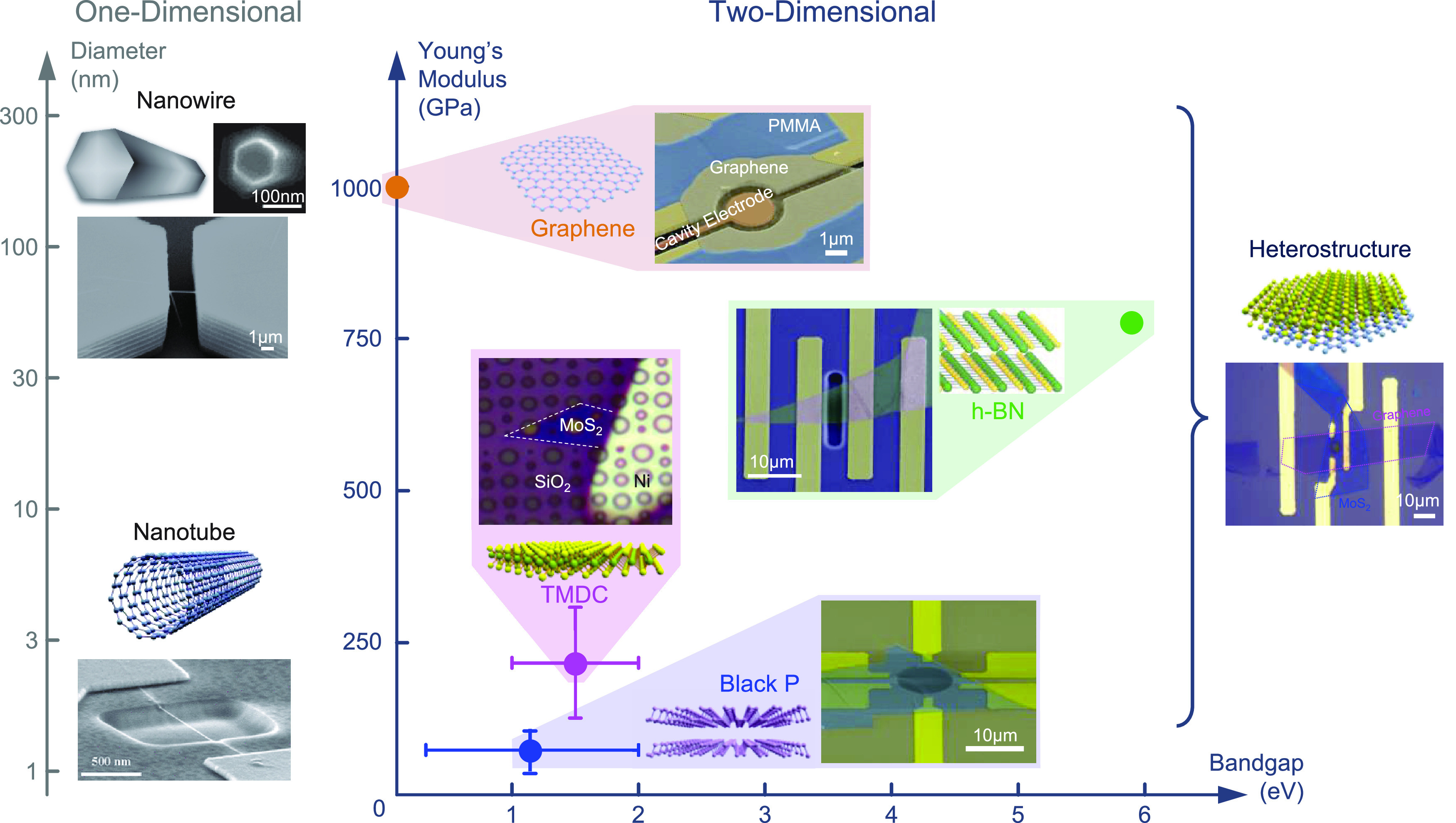
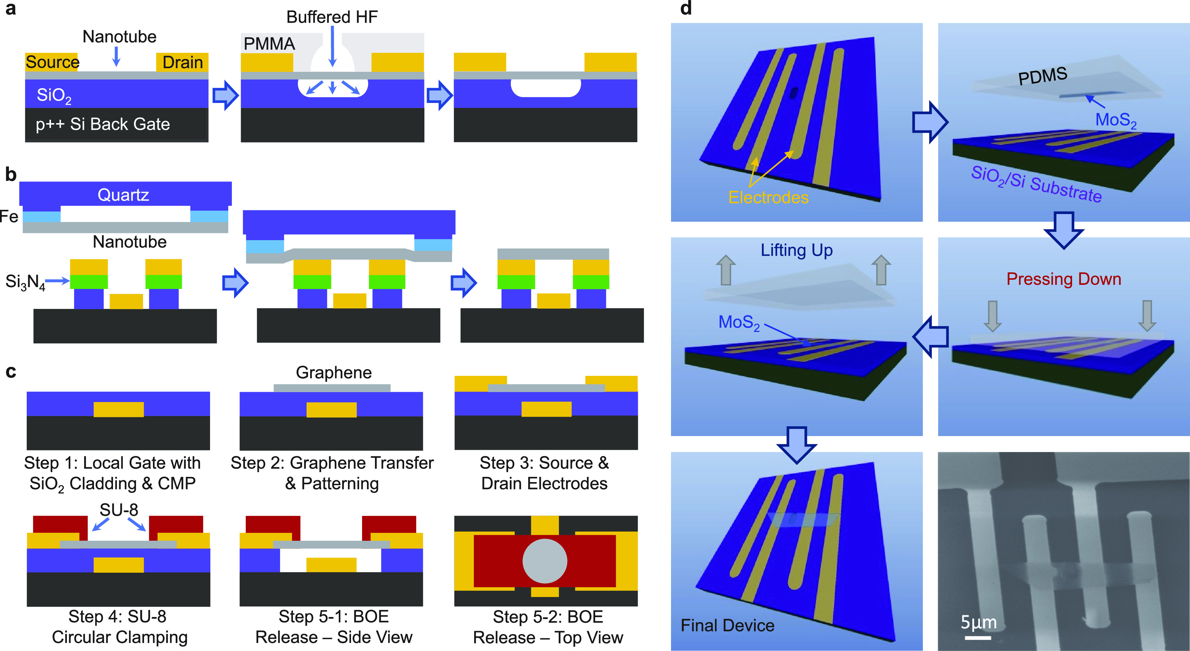
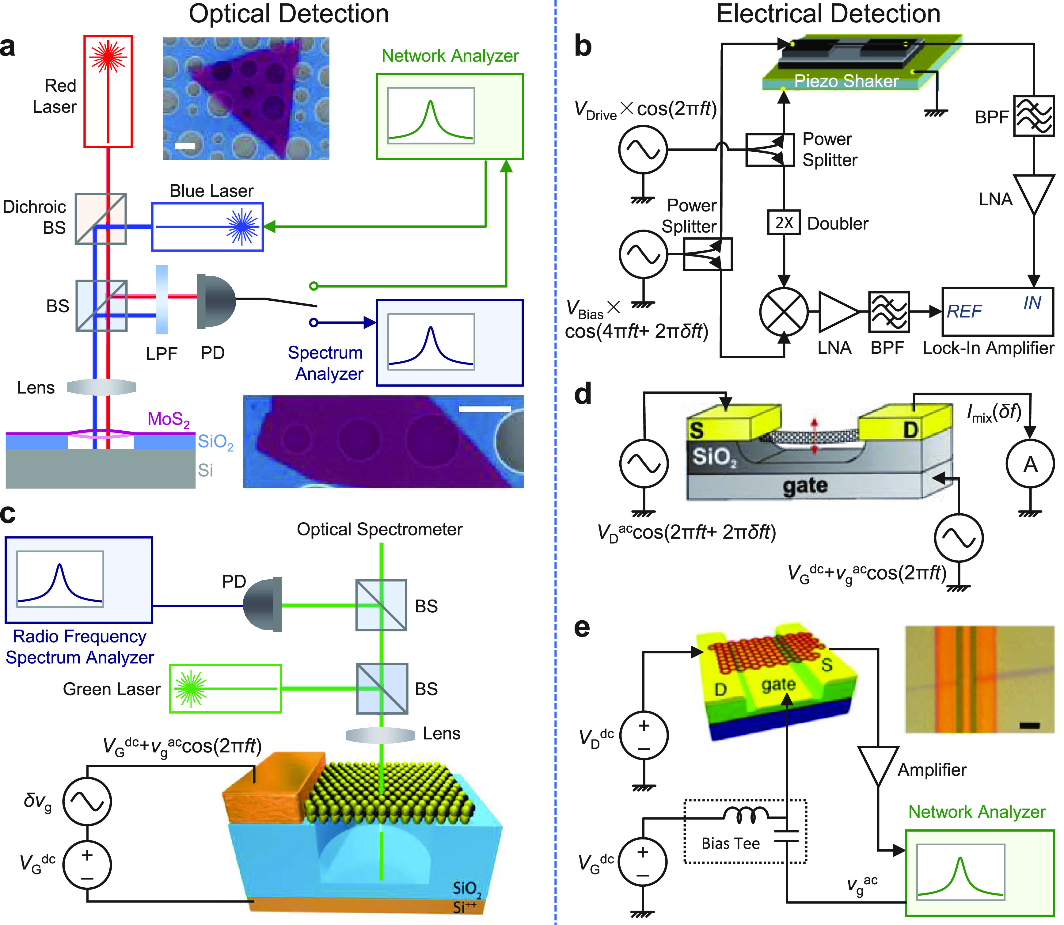
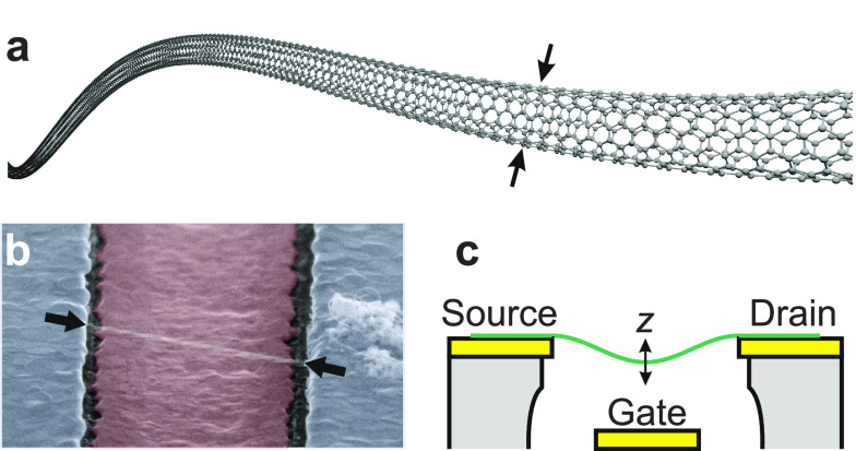
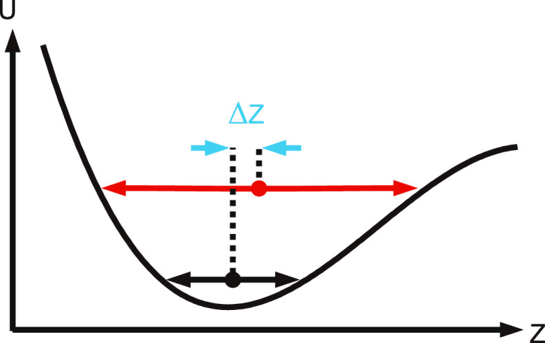
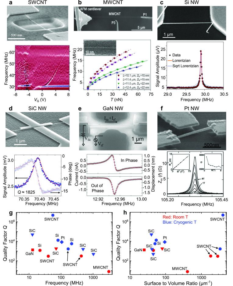
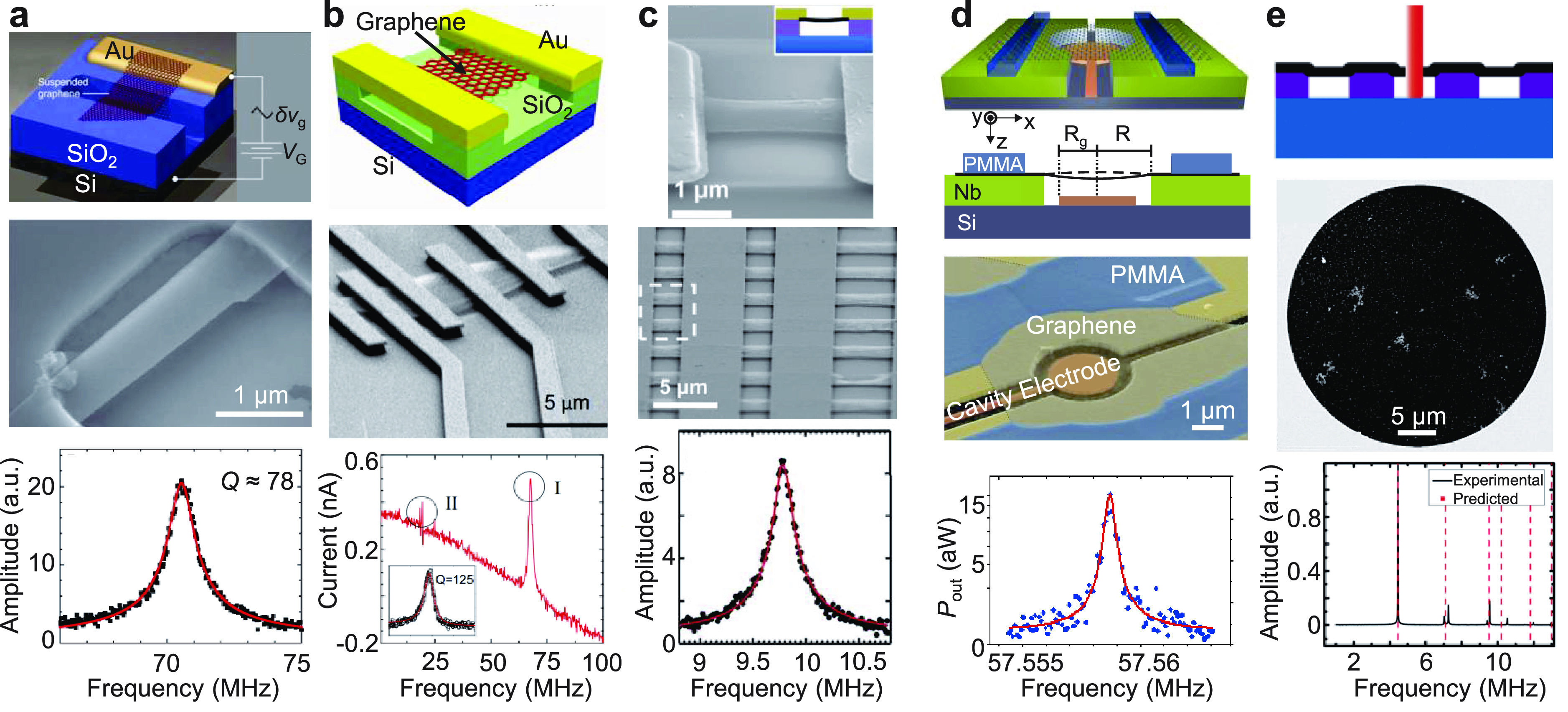
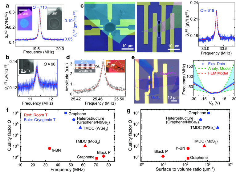
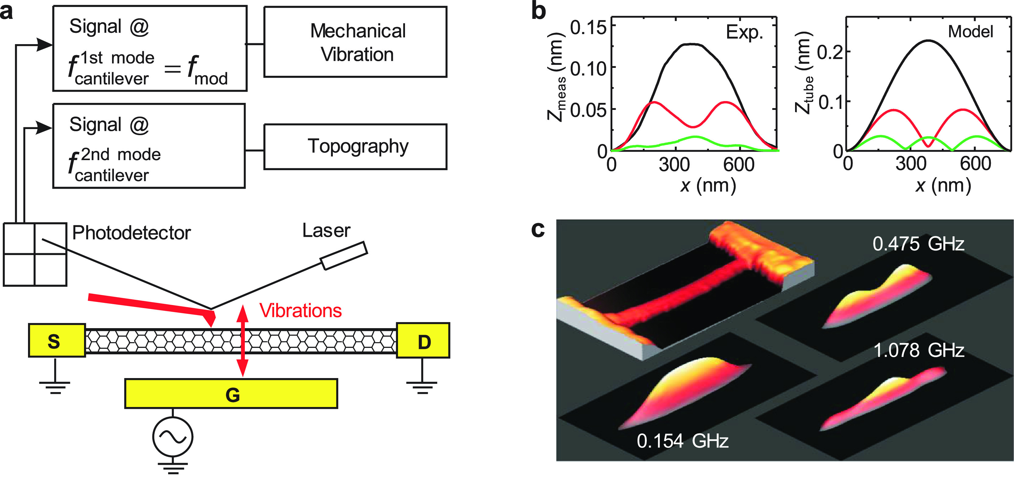
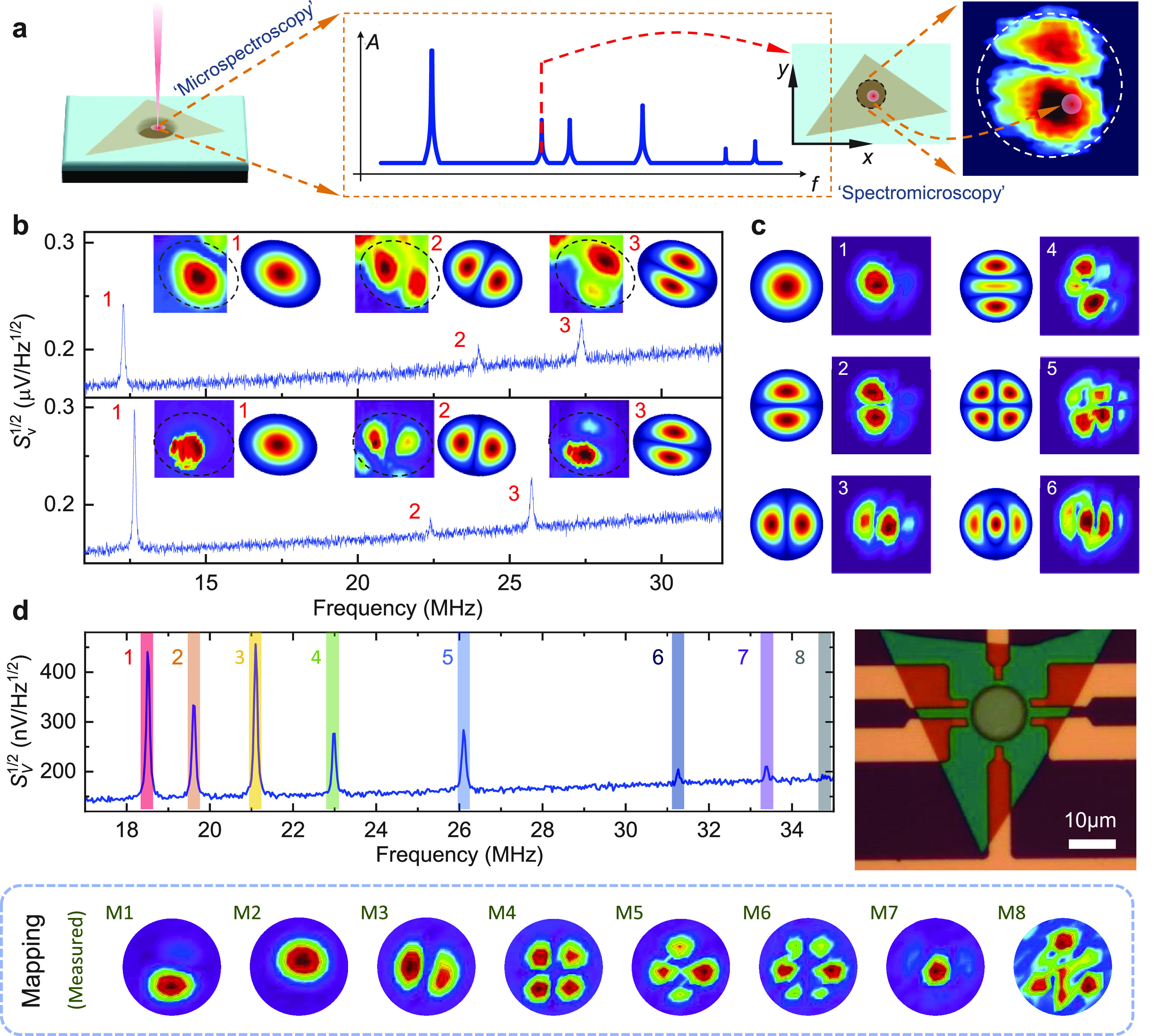
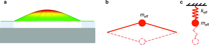
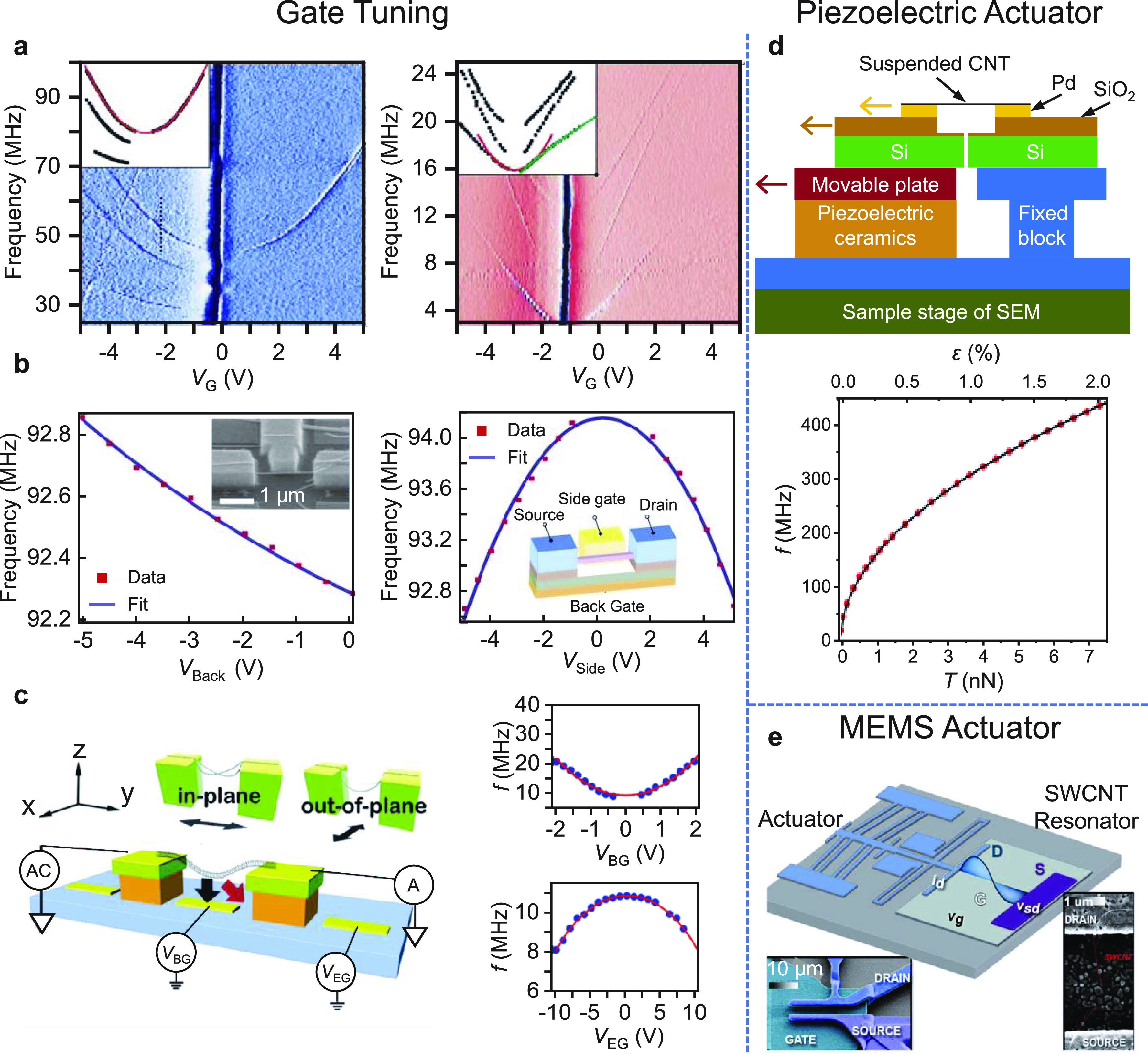
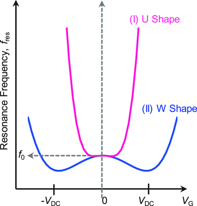
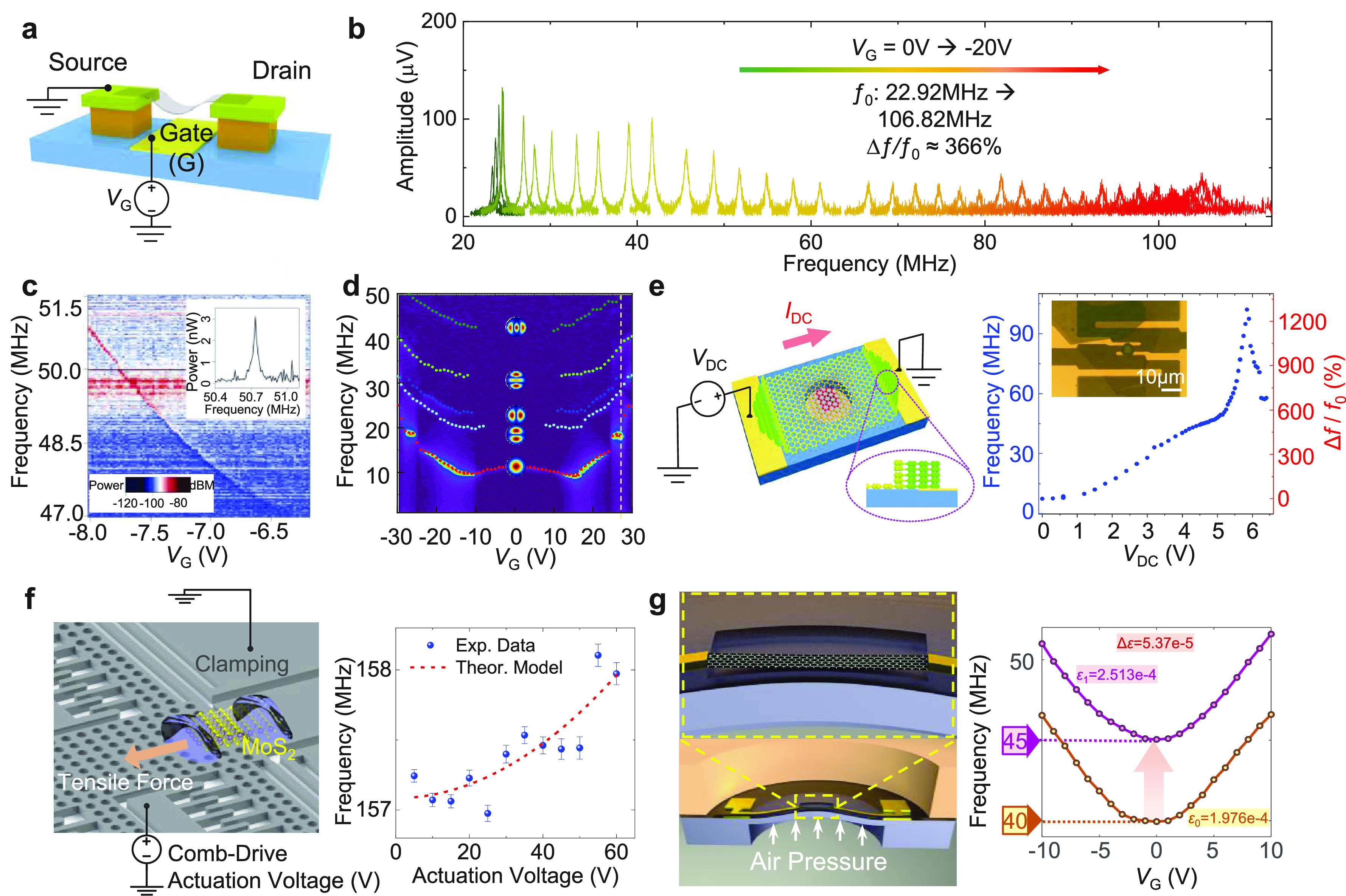
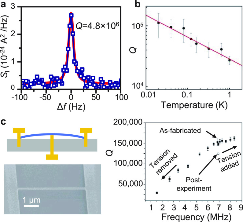
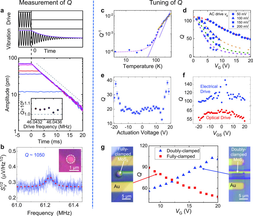
The quest for realizing and manipulating ever smaller man-made movable structures and dynamical machines has spurred tremendous endeavors, led to important discoveries, and inspired researchers to venture to previously unexplored grounds. Scientific feats and technological milestones of miniaturization of mechanical structures have been widely accomplished by advances in machining and sculpturing ever shrinking features out of bulk materials such as silicon. With the flourishing multidisciplinary field of low-dimensional nanomaterials, including one-dimensional (1D) nanowires/nanotubes and two-dimensional (2D) atomic layers such as graphene/phosphorene, growing interests and sustained effort have been devoted to creating mechanical devices toward the ultimate limit of miniaturization─genuinely down to the molecular or even atomic scale. These ultrasmall movable structures, particularly nanomechanical resonators that exploit the vibratory motion in these 1D and 2D nano-to-atomic-scale structures, offer exceptional device-level attributes, such as ultralow mass, ultrawide frequency tuning range, broad dynamic range, and ultralow power consumption, thus holding strong promises for both fundamental studies and engineering applications. In this Review, we offer a comprehensive overview and summary of this vibrant field, present the state-of-the-art devices and evaluate their specifications and performance, outline important achievements, and postulate future directions for studying these miniscule yet intriguing molecular-scale machines.

Keywords: dynamic range; frequency tuning; nanoelectromechanical systems; one-dimensional materials; quantum engineering; radio frequency; resonators; sensing; signal processing; two-dimensional materials.


Conflict of interest statement

The authors declare no competing financial interest.

Figures

Figure 1.1
Figure 1.1
Nanomechanical resonators enabled by diverse 1D and 2D nanomaterials. SEM images and optical images are reprinted in part with permission from ref (10), copyright 2007 American Chemical Society; from ref (19), copyright 2015 Royal Society of Chemistry; from ref (63), copyright 2018 The Authors, some rights reserved; exclusive licensee AAAS. Distributed under a CC BY-NC 4.0 license http://creativecommons.org/licenses/by-nc/4.0/; from ref (125), copyright 2014 American Chemical Society; from ref (179), copyright 2021 American Chemical Society; from ref (198), copyright 2006 American Chemical Society; and under a Creative Commons (CC BY) License from ref (20), copyright 2017 Springer Nature, respectively.
Figure 2.1
Figure 2.1
Schematic illustrations of fabrication processes for 1D and 2D NEMS resonators. (a) Suspending a nanotube by etching the sacrificial layer underneath using buffered hydrofluoric acid (HF) etching. Reprinted in part with permission from ref (198). Copyright 2013 American Chemical Society. (b) One-step direct transfer of CNTs for NEMS resonators and other functional devices. Reprinted in part with permission from ref (49). Copyright 2010 American Chemical Society. (c) Etching of sacrificial layer underneath graphene, with SU-8 circularly clamping the graphene to form a circular resonator with a local gate electrode. Reprinted in part with permission from ref (58). Copyright 2013 American Physical Society. (d) Dry transfer of molybdenum disulfide (MoS2) onto a substrate with predefined microtrenches and contact electrodes. Reprinted in part with permission from ref (61). Copyright 2014 AVS American Institute of Physics.
Figure 3.1
Figure 3.1
Nanomechanical resonance excitation and measurement techniques. (a) Schematic for optothermal excitation (blue laser) and optical interferometry readout (red laser) of 2D MoS2 resonators. Reprinted in part with permission from ref (63). Copyright 2018 The Authors, some rights reserved; exclusive licensee AAAS. Distributed under a CC BY-NC 4.0 license http://creativecommons.org/licenses/by-nc/4.0/. (b) Piezoelectric excitation and piezoresistive detection of Si NW resonators. Reprinted in part with permission from ref (72). Copyright 2008 American Chemical Society. (c) Schematic for capacitive excitation and optical interferometry readout of 2D tungsten disulfide (WSe2) resonators. Reprinted in part with permission under a Creative Commons (CC BY) License from ref (65). Copyright 2016 American Chemical Society. (d) Capacitive excitation and frequency down-mixing electrical readout of CNT resonators. Reprinted in part with permission from ref (110). Copyright 2009 American Association for the Advancement of Science. (e) Direct RF electrical readout of graphene resonators. Note the difference between the global gate design and the local gate design (as in d and e, respectively). Reprinted in part with permission from ref (87). Copyright 2010 American Institute of Physics. Panels (a) and (c) belong to optical detection, while panels (b), (d), and (e) belong to electrical detection.
Figure 4.1
Figure 4.1
Structure of CNTs and typical device geometry of a nanotube resonator. (a) Illustration of the atomic lattice forming a nanotube. Individual carbon atoms are shown as spheres and carbon–carbon bonds as lines. The distance between the arrows is the tube diameter. (b) Colored scanning electron micrograph showing a nanotube suspended over a trench. The gate electrode underneath the nanotube is shown in red. The arrows indicate the clamping points. Adapted with permission from ref (98). Copyright 2011 American Chemical Society. (c) Sketch of typical device geometry, with a nanotube (green) suspended freely between source and drain electrodes over a gate electrode and vibrating in z-direction. Metal electrodes are shown in yellow.
Figure 4.2
Figure 4.2
Sketch of an oscillation potential U(z) with a broken symmetry. Small and large oscillations have different equilibrium positions, see black and red lines. A change in the oscillation amplitude results in a static shift Δz. Reprinted in part with permission from ref (97). Copyright 2013 Springer Nature.
Figure 4.3
Figure 4.3
Examples of 1D NEMS resonators, with SEM images and representative resonance characteristics shown for (a) SWCNT, reprinted in part with permission from ref (198). Copyright 2006 American Chemical Society. (b) MWCNT, reprinted in part with permission from ref (116). Copyright 2009 Wiley-VCH Verlag. (c) Si NW, reprinted in part with permission from ref (72). Copyright 2008 American Chemical Society. (d) SiC NW, reprinted in part with permission from ref (117). Copyright 2009 Institute of Electrical and Electronics Engineers. (e) Gallium nitride (GaN) NW, reprinted in part with permission from ref (118). Copyright 2012 American Institute of Physics. (f) Pt NW NEMS resonators, reprinted in part with permission from ref (33). Copyright 2003 American Institute of Physics. (g) Measured Q vs resonance frequency for some of the 1D NEMS resonators. Data taken from refs (, , , , , , −, , , , and 254). (h) Measured Q vs surface-to-volume ratio for the same set of 1D NEMS resonators as in (g). In both (g) and (h), data measured at room temperature and cryogenic temperatures are shown in red and blue, respectively.
Figure 5.1
Figure 5.1
Graphene NEMS resonators with examples of device schematics, SEM images, and measured resonances, for (a) the first graphene NEMS resonator with optical interferometry readout. Reprinted in part with permission from ref (16). Copyright 2007 American Association for the Advancement of Science. (b) The first graphene NEMS resonator with electrical readout. Reprinted in part with permission from ref (57). Copyright 2009 Springer Nature. (c) A large-scale array of NEMS resonators made from CVD graphene. Reprinted in part with permission from ref (60). Copyright 2010 American Chemical Society. (d) A graphene resonator coupled to a superconducting microwave cavity. Reprinted in part with permission from ref (125). Copyright 2014 American Chemical Society. (e) CVD graphene resonators with diameter up to 30 μm showing size-dependent quality factor. Reprinted in part with permission from ref (123). Copyright 2011 American Chemical Society.
Figure 5.2
Figure 5.2
NEMS resonators based on 2D materials beyond graphene. (a) The first experimentally demonstrated MoS2 nanomechanical resonator, showing undriven thermomechanical motion. Reprinted in part with permission from ref (17). Copyright 2013 American Chemical Society. (b) The first black P NEMS resonator. Reprinted in part with permission from ref (19). Copyright 2015 Royal Society of Chemistry. (c) False-colored SEM images of circularly clamped and doubly clamped h-BN resonators as well as the undriven thermomechanical resonance spectra. Reprinted in part with permission under a Creative Commons (CC BY) License from ref (20). Copyright 2017 Springer Nature. (d) Resonant response of a NEMS resonator based on 2D antiferromagnets chromium triiodide (CrI3) encapsulated by WSe2 and graphene. Reprinted in part with permission from ref (21). Copyright 2020 Springer Nature. (e) NEMS resonator based on 2D atomic layer van der Waals HS and gate tuning of its resonance frequency. Reprinted in part with permission from ref (179). Copyright 2021 American Chemical Society. (f) Measured Q vs resonance frequency for some representative 2D NEMS resonators. Data taken from refs (, , , , , , and 154). (g) Measured Q vs surface-to-volume ratio for the same set of 2D NEMS resonators as in (f). In both (f) and (g), data measured at room temperature and cryogenic temperatures are shown in red and blue, respectively. Some representative data from graphene NEMS are included in (f) and (g) for reference.
Figure 6.1
Figure 6.1
Visualizing motion and mode shapes in 1D NEMS resonators. (a) Schematic illustration of mode shape mapping for a CNT resonator. (b) Measured and simulated mode shapes for the first three modes. (c) 3D illustration of the measured mode shapes. Reprinted in part with permission from ref (74). Copyright 2007 American Physical Society.
Figure 6.2
Figure 6.2
Visualizing motion and mode shapes in 2D NEMS resonators. (a) Schematic illustration of mode shape mapping in 2D NEMS resonators. (b) Spatial mapping of a MoS2 resonator with structural nonidealities. Reprinted in part with permission from ref (170). Copyright 2014 Springer Nature. (c) Comparison of the spatially resolved mode shapes with simulation for an anisotropic black P resonator. Reprinted in part with permission from ref (136). Copyright 2016 American Chemical Society. (d) An h-BN resonator device image, measured thermomechanical resonance spectrum with 8 resonance modes, and spatial mapping of the 8 modes. Reprinted in part with permission under a Creative Commons (CC BY) License from ref (20). Copyright 2017 Springer Nature.
Figure 7.1
Figure 7.1
Mechanical model of a 2D resonator. (a) Schematic illustration (side view) of a fully clamped 2D NEMS resonator in its fundamental mode. (b) A simplified version of the resonator showing the vibration of the effective mass. (c) The lumped parameter model of the resonator in a spring-mass system.
Figure 7.2
Figure 7.2
Frequency tuning in 1D NEMS resonators. (a) Observation of gate tuning of the resonance frequency in CNT resonators. Reprinted in part with permission from ref (11). Copyright 2010 Nature Publishing Group. (b) Capacitive softening and spring hardening in an SnO2 NW, by sweeping the voltage on the back gate (left) or the side gate (right). Reprinted in part with permission from ref (36). Copyright 2009 American Institute of Physics Publishing. (c) Capacitive softening and spring hardening in a CNT resonator, by choosing the out-of-plane mode (top) or the in-plane mode (bottom). Reprinted in part with permission from ref (173). Copyright 2011 American Chemical Society. (d) Frequency tuning of CNT resonators using a piezoelectric actuator. Reprinted in part with permission from ref (12). Copyright 2014 American Chemical Society. (e) Axially tunable CNT resonators using cointegrated microactuators. Reprinted in part with permission from ref (111). Copyright 2014 American Chemical Society.
Figure 7.3
Figure 7.3
Schematic illustrations of tuning curves of “U-shape” and “W-shape” in 1D or 2D NEMS resonators. Reprinted in part with permission from ref (63). Copyright 2018 The Authors, some rights reserved; exclusive licensee AAAS. Distributed under a CC BY-NC 4.0 license http://creativecommons.org/licenses/by-nc/4.0/.
Figure 7.4
Figure 7.4
Frequency tuning in 2D NEMS resonators. (a) Schematic illustration of a doubly clamped 2D resonator, with deformation and strain induced by DC gate voltage. (b) Gate tuning of the resonance frequency for a 2D HS resonator. Reprinted in part with permission from ref (179). Copyright 2021 American Chemical Society. (c) Color plot of frequency tuning via DC gate voltage in a graphene NEMS oscillator. Reprinted in part with permission from ref (59). Copyright 2013 Nature Publishing Group. (d) Multimode resonances frequency tuning in a black P resonator. Reprinted in part with permission from ref (136). Copyright 2016 American Chemical Society. (e) Schematic of Joule heating in a fully clamped 2D resonator, and frequency tuning of a graphene resonator (inset) using Joule heating. Reprinted in part with permission from ref (258), copyright 2018 American Chemical Society, and ref (181), copyright 2018 Institute of Electrical and Electronics Engineers. (f) Illustration of a comb-drive actuator controlling strain in a doubly clamped MoS2 resonator, and the measured frequency tuning data at different comb-drive actuation voltages. Reprinted in part with permission from ref (183). Copyright 2021 Wiley-Blackwell. (g) Schematic illustration for tuning the strain in a graphene resonator by deforming the membrane using pressure difference. Reprinted in part with permission from ref (245). Copyright 2021 Institute of Physics.
Figure 8.1
Figure 8.1
Controlling and enhancing Q in 1D NEMS resonators. (a) Resonance spectrum of a CNT resonator showing Q close to 5 million. Reprinted in part with permission from ref (104). Copyright 2014 Nature Publishing Group. (b) Temperature dependence of Q in a CNT resonator. Reprinted in part with permission from ref (40). Copyright 2009 American Chemical Society. (c) Strain tuning of Q and f in a silicon nitride NW resonator by substrate bending. Reprinted in part with permission from ref (199). Copyright 2007 American Chemical Society.
Figure 8.2
Figure 8.2
Controlling and enhancing Q in 2D NEMS resonators. (a) A graphene resonators measured at 15 mK, showing Q exceeding 1 million. Reprinted in part with permission from ref (142). Copyright 2021 Springer Nature. (b) Thermomechanical resonance of a 2D MoS2 resonator measured at room temperature, showing Q exceeding 1000. Reprinted in part with permission from ref (63). Copyright 2018 The Authors, some rights reserved; exclusive licensee AAAS. Distributed under a CC BY-NC 4.0 license http://creativecommons.org/licenses/by-nc/4.0/. (c) Temperature dependence of Q for a 2D MoS2 resonator. Reprinted in part with permission under a Creative Commons (CC-BY-NC-ND) License from ref (205). Copyright 2017 Nature Publishing Group. (d) Dependence of Q on DC and AC gate voltages, for 2D MoS2 NEMS resonators. Reprinted in part with permission from ref (208). Copyright 2022 American Chemical Society. (e) Q vs comb-drive actuation voltage for 2D MoS2 resonator mounted on a comb-drive. Reprinted in part with permission from ref (183). Copyright 2021 Wiley-Blackwell. (f) Gate tuning of Q for MoS2 resonators. Reprinted in part with permission from ref (63). Copyright 2018 The Authors, some rights reserved; exclusive licensee AAAS. Distributed under a CC BY-NC 4.0 license http://creativecommons.org/licenses/by-nc/4.0/. (g) Different effect of tuning Q for fully clamped and doubly clamped 2D MoS2 NEMS resonators using DC gate voltage. Reprinted in part with permission from ref (208). Copyright 2022 American Chemical Society.
Figure 9.1
Figure 9.1
Nonlinearity and DR in 1D and 2D NEMS resonators. (a) Definition of DR in a NEMS resonator, from thermomechanical resonance to onset of nonlinearity as vibration amplitude increases. Reprinted in part with permission from ref (218). Copyright 2014 American Institute of Physics. (b) Resonance spectra of the doubly clamped SiC NW resonator with increasing drive, showing Duffing nonlinearity. Reprinted in part with permission from ref (172). Copyright 2006 American Institute of Physics. (c) Nonlinear damping in a CNT resonator. Reprinted in part with permission from ref (101). Copyright 2011 Nature Publishing Group. (d) Calculated DR for doubly clamped 1D NEMS resonators with different lengths, including CNT and NW resonators. Reprinted in part with permission from ref (95). Copyright 2005 American Institute of Physics. (e) Calculated DR for fully clamped circular 2D NEMS resonators at 300 K. Reprinted in part with permission from ref (218). Copyright 2014 American Institute of Physics. (f) Softening and hardening nonlinearities measured in monolayer and 3-layer 2D MoS2 NEMS resonators as well as DRs. Reprinted in part with permission from ref (63). Copyright 2018 The Authors, some rights reserved; exclusive licensee AAAS. Distributed under a CC BY-NC 4.0 license http://creativecommons.org/licenses/by-nc/4.0/.
Figure 10.1
Figure 10.1
Coupled resonators. (a) Schematic illustration of two coupled modes in a spring-mass model. (b) Illustration of two singly clamped beam resonators coupled through a coupling beam. (c) Illustration of two singly clamped beam resonators coupled through a common clamping edge. In both (b) and (c), the origin of the coupling spring term kc is indicated.
Figure 10.2
Figure 10.2
Internal resonance and frequency pinning in an MoS2 NEMS resonator. (a) The frequency response of the device with positive Duffing nonlinearity. (b) Pinning of the jump-down frequency when the internal resonance occurs in the multistable regime. Reprinted in part with permission from ref (132). Copyright 2015 American Institute of Physics.
Figure 10.3
Figure 10.3
Internal resonance in a CNT resonator. (a) Nonlinear resonant coupling revealed by measuring the oscillation amplitude of a single mode with the two-source current mixing method as a function of gate voltage VG. The measured current ranges from 0 (black) to 1 nA (red). An avoided crossing is observed when the frequency is half that of a higher-order mode. Reprinted in part with permission from ref (94). Copyright 2012 American Physical society. (b–e) Response of the vibration amplitude (which is roughly proportional to the current) to an oscillating force at different gate voltages indicated by the symbols in (a). Black and red lines are sweeps with increasing and decreasing frequency, respectively. The line shapes are highly irregular due to an interplay of nonlinear resonant coupling and nonlinear Duffing response oscillations. Reprinted in part with permission from ref (94). Copyright 2012 American Physical society.
Figure 10.4
Figure 10.4
Parametric coupling in NEMS resonators. (a) Illustration of a red-detuned pump alongside the two coupled modes in the frequency domain. (b, c) The response of mode 1 as a function of the red-pump detuning when Vp = 0 V (b) and Vp = 1.5 V (c) in a graphene drumhead resonator. For nonzero pump amplitudes, mode 1 is seen to split in the vicinity of ωp ≈ |ω1 – ω2|. Inset, the response detected at ωd + ωp. Energy transfer to the second mode is seen when ωd + ωp ≈ ω2. (d) Response of mode 1 at fine intervals of the pump voltage. (e) Cooperativity, a figure of merit that quantifies the magnitude of intermodal coupling vs pump amplitudes. The solid line is a quadratic fit of the data (circles) to the equation C = αVp2. (f) Higher-order parametric coupling in NEMS resonators: Mode 1 response as a function of the pump detuning over a larger frequency range in a graphene drumhead resonator. Apart from normal mode splitting at ωp ≈ Δω = |ω1 – ω2|, an extra splitting at ωp ≈ (Δω)/2 can be seen, suggesting the onset of higher-order intermodal coupling. (a–f) Reprinted in part with permission from ref (227). Copyright 2016 Nature Publishing Group.
Figure 11.1
Figure 11.1
Mass sensing applications using NEMS resonators. (a) Schematic illustration of Xe atom mass sensing using a SiC NW resonator and the measured frequency response to mass loading, showing zg-level mass sensing. Reprinted in part with permission from ref (247). Copyright 2011 American Chemical Society. (b) SEM image and resonance curve during adsorption for a CNT resonator. Reprinted in part with permission from ref (71). Copyright 2008 American Chemical Society. (c) SEM image and mass sensing data for a CNT resonator, showing down to 1.7 yoctogram resolution. Reprinted in part with permission from ref (250). Copyright 2012 Nature Publishing Group. (d) Schematic illustration of fluctuation of Xe atoms (including adsorption, desorption, and surface diffusion) on a SiC NW resonator. Reprinted in part with permission from ref (247). Copyright 2011 American Chemical Society. (e) Low-dimensional phase transition of Kr atoms adsorbed on the surface of a CNT resonator, detected by monitoring the resonance frequency. Reprinted in part with permission from ref (42). Copyright 2010 American Association for the Advancement of Science. (f) Mass sensing behavior of graphene resonator. Reprinted in part with permission from ref (57). Copyright 2009 Nature Publishing Group.
Figure 11.2
Figure 11.2
Force sensing applications of low-dimensional NEMS resonators. (a) AFM image of a 4 μm long CNT, schematic of the device, and the corresponding force sensing experimental results showing zN force sensing at 1.2 K and 3 K. Reprinted in part with permission from ref (91). Copyright 2013 Nature Publishing Group. (b) False-colored image of a multilayer graphene resonator and the force sensitivity under different numbers of pump photons. Reprinted in part with permission under a Creative Commons (CC BY) License from ref (77). Copyright 2016 Nature Publishing Group.
Figure 11.3
Figure 11.3
Various sensing applications demonstrated using low-dimensional NEMS resonators. (a) Schematic illustration of a 2D MoS2 resonator used for γ-ray radiation sensing and the measured sensing data. Reprinted in part with permission from ref (260). Copyright 2016 American Institute of Physics. (b) Schematic illustration of a graphene accelerometer and sensing data. Reprinted in part with permission from ref (261). Copyright 2019 Nature Publishing Group. (c) Schematics of the cross section of a MoS2 resonator at different pressures, and the measured dependence of the resonance frequency on chamber pressure. Reprinted in part with permission from ref (263). Copyright 2014 Institute of Electrical and Electronics Engineers.
Figure 12.1
Figure 12.1
Low-dimensional NEMS resonators for RF signal processing. (a) False-colored SEM images of self-sustained SiC NW NEMS oscillators, the corresponding measurement circuit diagram showing a feedback loop, and the clean, stable, sinusoidal time-domain oscillation waveform of the oscillators. Reprinted in part with permission from ref (115). Copyright 2008 Nature Publishing Group. (b) False-colored SEM image of a circular graphene oscillator with SU-8 clamp and local gate electrodes, the simplified circuit for a graphene radio station, and the transmitted and received audio waveform of 1 s soundtrack from the graphene NEMS oscillator. Reprinted in part with permission from ref (59). Copyright 2013 Nature Publishing Group. (c) SEM images of a CNT resonator, FM mixing and demodulation circuit, and the measurement data showing the feasibility of digital demodulation using CNT resonator. Reprinted in part with permission from ref (70). Copyright 2010 Wiley-VCH.
Figure 12.2
Figure 12.2
Advanced coupled NEMS devices. (a) Schematic of a graphene-based acoustic waveguide, where the graphene film is suspended over a trench with a gate electrode array at its bottom. Reprinted in part with permission from ref (222). Copyright 2019 American Physical Society. (b) Schematic of an h-BN phononic crystal waveguide. Reprinted in part with permission from ref (223). Copyright 2019 American Chemical Society. (c) Schematic of a graphene/silicon nitride hybrid resonant structure. Reprinted in part with permission from ref (224). Copyright 2020 American Chemical Society. (d) Giant tunable mechanical nonlinearity in a graphene–silicon nitride hybrid resonator. Reprinted in part with permission from ref (225). Copyright 2020 American Chemical Society.
Figure 12.3
Figure 12.3
CNT resonator as a quantum dot. (a) Sketch of a CNT coupled to source and drain leads with charge transport rates ΓS,D. The total electrical charge of the nanotube can be tuned capacitively by a gate voltage. The nanotube-gate capacitance CG(z) depends on the nanotube displacement z. (b) Electrical conductance and mechanical resonance frequency as a function of the gate voltage measured at a temperature of 16 K. Reprinted in part with permission from ref (272). Copyright 2014 Nature Publishing Group.
Figure 12.4
Figure 12.4
Mechanical resonant frequency in a graphene resonator as functions of the applied magnetic fields at different VG and corresponding fits (red curves). Reprinted in part with permission from ref (282). Copyright 2016 Nature Publishing Group.
Figure 12.5
Figure 12.5
Parametric sideband cooling in a graphene resonator. (a) Schematic of the experimental setup. (b) Schematic of sideband pumping in frequency space. The curved arrows indicate the direction of energy flow when the system is pumped at ωp. (c) Amplification of a mode as another mode is pumped at its Stokes sideband. (d) Parametric cooling in a mode on pumping the anti-Stokes sideband of another mode. (a–d) Reprinted in part with permission from ref (228). Copyright 2016 Nature Publishing Group.
Figure 13.1
Figure 13.1
Artistic illustration of a 2D NEMS resonator integrated with a CMOS circuit.

References

    1. Richards V. Molecular Machines. Nat. Chem. 2016, 8, 1090–1090. 10.1038/nchem.2687. - DOI - PubMed
    1. Browne W. R.; Feringa B. L. Making Molecular Machines Work. Nat. Nanotechnol. 2006, 1, 25–35. 10.1038/nnano.2006.45. - DOI - PubMed
    1. Lancia F.; Ryabchun A.; Katsonis N. Life-Like Motion Driven by Artificial Molecular Machines. Nat. Rev.Chem. 2019, 3, 536–551. 10.1038/s41570-019-0122-2. - DOI
    1. Berná J.; Leigh D. A.; Lubomska M.; Mendoza S. M.; Pérez E. M.; Rudolf P.; Teobaldi G.; Zerbetto F. Macroscopic Transport by Synthetic Molecular Machines. Nat. Mater. 2005, 4, 704–710. 10.1038/nmat1455. - DOI - PubMed
    1. Abendroth J. M.; Bushuyev O. S.; Weiss P. S.; Barrett C. J. Controlling Motion at the Nanoscale: Rise of the Molecular Machines. ACS Nano 2015, 9, 7746–7768. 10.1021/acsnano.5b03367. - DOI - PubMed