. 2022 Nov;9(32):e2202695.
doi: 10.1002/advs.202202695. Epub 2022 Sep 11.

2+δ-Dimensional Materials via Atomistic Z-Welding

Affiliations

2+δ-Dimensional Materials via Atomistic Z-Welding

Tumesh Kumar Sahu et al. Adv Sci (Weinh). 2022 Nov.

Abstract

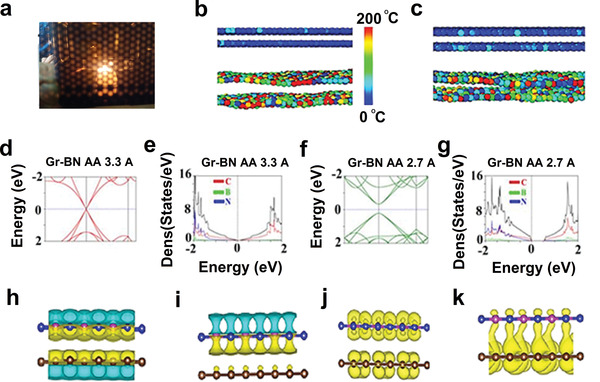
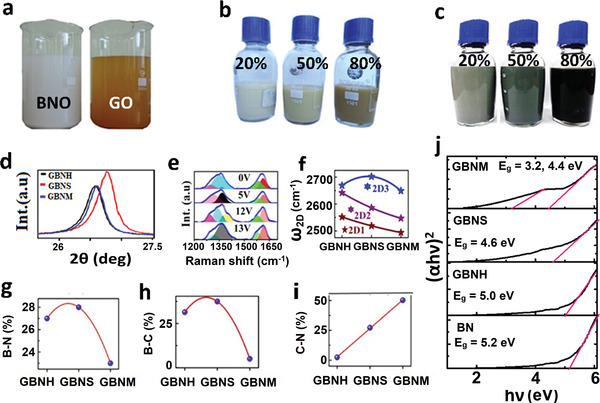
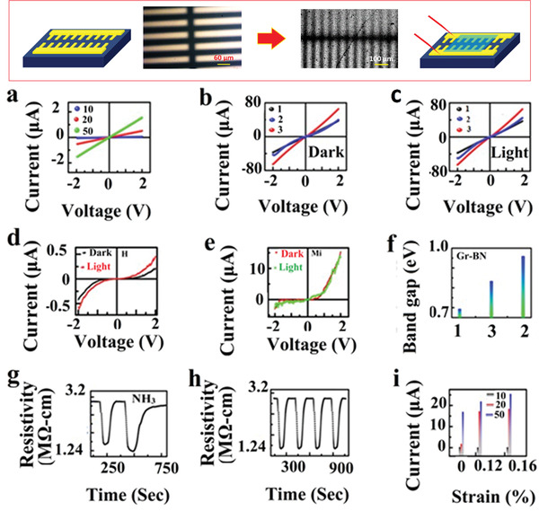
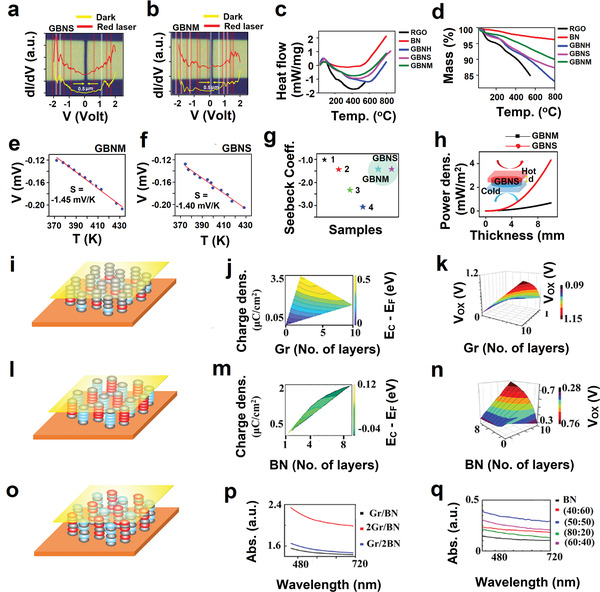
Pivotal to functional van der Waals stacked flexible electronic/excitonic/spintronic/thermoelectric chips is the synergy amongst constituent layers. However; the current techniques viz. sequential chemical vapor deposition, micromechanical/wet-chemical transfer are mostly limited due to diffused interfaces, and metallic remnants/bubbles at the interface. Inter-layer-coupled 2+δ-dimensional materials, as a new class of materials can be significantly suitable for out-of-plane carrier transport and hence prompt response in prospective devices. Here, the discovery of the use of exotic electric field ≈106 V cm- 1 (at microwave hot-spot) and 2 thermomechanical conditions i.e. pressure ≈1 MPa, T ≈ 200 °C (during solvothermal reaction) to realize 2+δ-dimensional materials is reported. It is found that Pz Pz chemical bonds form between the component layers, e.g., CB and CN in G-BN, MoN and MoB in MoS2 -BN hybrid systems as revealed by X-ray photoelectron spectroscopy. New vibrational peaks in Raman spectra (BC ≈1320 cm-1 for the G-BN system and MoB ≈365 cm-1 for the MoS2 -BN system) are recorded. Tunable mid-gap formation, along with diodic behavior (knee voltage ≈0.7 V, breakdown voltage ≈1.8 V) in the reduced graphene oxide-reduced BN oxide (RGO-RBNO) hybrid system is also observed. Band-gap tuning in MoS2 -BN system is observed. Simulations reveal stacking-dependent interfacial charge/potential drops, hinting at the feasibility of next-generation functional devices/sensors.

Keywords: 2+ δ dimensional; 2D materials; hybridization; hydrothermal; microwave.


Conflict of interest statement

The authors declare no conflict of interest.

Figures

Figure 1
Figure 1
a) Schematic diagram of sonochemical hybridization process. b) TEM image for 1 wt% of Gr‐BN and its HRTEM images in overlap areas marked in TEM as 1 and 2, insets corresponding to their FFT pattern. c) TEM image for 0.5 wt% Gr‐BN system overlapped areas confirmed by elemental mapping marked as 1 and 2 and their HRTEM images, in inset corresponding FFT patterns f) bandgap histogram for hybrid systems with different wt% (0 to 5 wt%) of Gr in BN obtained from UV‐visible measurements and d) Raman spectra for hybrids (0.5 to 1) wt% of Gr in BN and e) deconvolution of 2D peaks for hybridized (0.5 and 1 wt%) samples.
Figure 2
Figure 2
Schematic diagram of hybridization approaches, HRTEM image, and zoomed‐in images for a) GBNH, b) GBNS, c) GBNM. Hexagonal symmetry is found in individual atomic sheets of G and BN. In hybrids, new symmetries evolve and mixed symmetries are found. To resolve local structural features, zoomed‐in images are shown. Interesting structural patterns of atoms are registered. Microwave (P+T+E) technique exhibits intense hybridization followed by the solvothermal (P+T) technique and heating (T) had the least effect. d) Schematic showing evolution of moire patterns at various angles between G and BN. Stripes, linear chains, circular (single) array, tricircle joining each other and various other features are generated at different angles.
Figure 3
Figure 3
a) Camera photo of the plasma generated during microwave processing. b) Molecular dynamics simulation for Gr‐BN solvothermally hybridized sample at equilibrium condition with average interlayer distance 3.3 Å and c) when hybridized, their interlayer distance locally decreased to 2.7 Å (color index exhibits localized temperature of the atoms). d) DFT band structure calculation for reduced Gr‐BN system considering AA stacking with interlayer distance 3.3 Å and e) DOS calculation for the Gr‐BN system with an insignificant band gap opening. f) DFT band structure calculation for AA stacking for Gr‐BN system with interlayer distance 2.7 Å in E‐k diagram exhibits parabolic dispersion with band gap opening and g) DOS calculation when the interlayer distance was 2.7 Å with AA stacking for Gr‐BN system which exhibits bandgap of 0.5 eV. h,i) Top and side views of charge density difference profile for Gr‐BN system in AA sequence with equilibrium distance 3.3 Å (electron transferred from Pz orbitals of Gr to Pz orbitals of BN). j,k) Charge density difference profile for reduced Gr‐BN system in AA stacking sequence with reduced distance 2.7 Å electron transfer from Pz orbitals of RGO to Pz orbitals of RBNO with physical bond formation due to strong interlayer coupling.
Figure 4
Figure 4
a) Camera images of BNO and GO as synthesized by modified Hummer's method. b) Typical GBNH samples with 20%, 50%, and 80% of RGO in RBNO. c) Typical GBNM samples with 20%, 50%, and 80% of RGO in RBNO. d) XRD, e) electric field‐dependent modulation of Raman spectra of 50:50 GBNM hybrid. f) 2D sub‐peaks (deconvoluted) positions, g) B‐N %, h) B‐C %, and i) C‐N % attained by XPS analysis in GBNH, GBNS, and GBNM samples. j) Tauc plot for BN, GBNH, GBNS, and GBNM samples.
Figure 5
Figure 5
a) Two probe IV measurements of hybridized RGO‐RBNO wt% at (10, 20, and 50) samples spin‐coated on PET substrate, conductivity increased with increasing % of RGO in BN from 0.1 to 1.8 µA. b,c) In‐plane IV measurements with and without a light source for (GBNH, GBNS, GBNM) hybridized samples, GBNM hybrid exhibited the highest current values 65 µA with semiconducting nature compared to GBNS (40 µA) and GBNH (35 µA), and the highest photocurrent response was recorded for GBNS ≈46 µA. d,e) IV measurements out‐of‐plane for GBNM and GBNS exhibited tunneling currents of 15 and 0.3 µA in the dark; upon exposure to blue light, it exhibited current values of 12 and 0.5 µA with semiconducting behavior. f) Electronic band gaps were calculated from R versus T measurement, highest bandgap was obtained for the GBNS sample of 0.96 eV compared to 0.83 eV for GBNM and 0.69 eV for the GBNH sample. g,h) Gas sensing behavior of hybridized RGO‐RBNO sample was studied upon exposure of analyte ammonia gas at different concentrations (70 and 100 PPM). Its repeatability behavior was demonstrated for five cycles at 70 PPM. i) Straintronics behavior was recorded for hybridized RGO‐RBNO samples (10, 20, and 50) wt% for spin‐coated on PET substrate, 50% RGO in BN sample exhibited the highest current from 2 to 17 µA when strain changed from 0% to 0.16%. Optical and SEM images of the device used for electrical measurements are shown in the top panel.
Figure 6
Figure 6
Optical image of the electrodes having separation of 0.5 µm and its quantum state measurements in the dark and with excitation of red laser light for a) GBNS and b) GBNM. c) DSC measurements for GBNS, GBNM, GBNH, RGO, and BN. d) TGA measurements for GBNS, GBNM, GBNH, RGO, and BN. e,f) Thermal conductivity measurements for GBNM and GBNS. g) Seebeck coefficient comparison of GBNS and GBNM with various samples 1‐pristine ϒ‐graphyne, 2‐ϒ graphyne with BN at the chain, 3‐ϒ graphyne with BN at the ring, and 4‐ϒ graphyne like BN sheets.[ 59 ] h) Simulation result of thermoelectric output power density with the variation of thickness of coating materials for GBNS and GBNM hybrid materials. i) Schematic diagram of Au/Gr/BN/Gr/Au device structure for tunneling current measurement, where Gr layer varies from 1 to 10 layer. j) Simulated charge density and energy difference between E c and E F (E CE F (eV)) in hybrid Au/Gr/BN/Gr/Au system by changing the number of Gr layers from monolayer to 10 layers, carrier density decreased from 3.82 to 1.56 µC cm2 and the energy difference between E C and E F decreased from 0.56 to 0.36 eV. k) The potential drop across dielectric (V ox) for interface fell from 0.42 to 0.1 V, with increasing Gr layer from monolayer to 10 layers. l) Schematic diagram of tunneling device Au/Gr/BN/Gr/Au structure for tunneling current measurement, where BN layer varies from 1 to 10 layers. m) Varying layer numbers, monolayer to 10 layers of BN charge carrier density increased from 0.008 to 2.2 µC cm2 and the energy difference between E C and E F (E CE F (eV)) decreased from 0.12 to −0.06 eV. n) The potential drop across the dielectric layer increased from 0.2 to 0.76 V by changing the BN layer number (1–10). o) Schematic diagram of Gr/BN/Gr, BN/Gr/BN used for UV‐vis spectra simulation p) simulated UV‐Visible spectra for Gr/BN with varying numbers of the layer. q) UV‐vis spectra for microwave‐hybridized RGO‐RBNO samples with different wt% of RGO on RBNO and compared with simulation results.

References

    1. Summerfield A., Kozikov A., Cheng T. S., Davies A., Cho Y.‐J., Khlobystov A. N., Mellor C. J., Foxon C. T., Watanabe K., Taniguchi T., Eaves L., Novoselov K. S., Novikov S. V., Beton P. H., Nano Lett. 2018, 18, 4241. - PMC - PubMed
    1. Kirill B. I., Ghahari F., Shulman M. D., Stormer H. L., Kim P., Nature 2009, 462, 196. - PubMed
    1. Srivastav S. K., Sahu M. R., Watanabe K., Taniguchi T., Banerjee S., Das A., Sci. Adv. 2019, 5, 5798. - PMC - PubMed
    1. Bolotin K. I., Sikes K. J., Jiang Z., Klima M., Fudenberg G., Hone J., Kim P., Stormer H. L., Solid State Commun. 2008, 146, 351.
    1. Dean C. R., Young A. F., Meric I., Lee C., Wang L., Sorgenfrei S., Watanabe K., Taniguchi T., Kim P., Shepard K. L., Hone J., Nat. Nanotechnol. 2010, 5, 722. - PubMed

LinkOut - more resources