. 2022 Sep 28;22(18):7457-7466.
doi: 10.1021/acs.nanolett.2c02395. Epub 2022 Sep 15.

Combining Freestanding Ferroelectric Perovskite Oxides with Two-Dimensional Semiconductors for High Performance Transistors

Affiliations

Combining Freestanding Ferroelectric Perovskite Oxides with Two-Dimensional Semiconductors for High Performance Transistors

Sergio Puebla et al. Nano Lett. .

Abstract

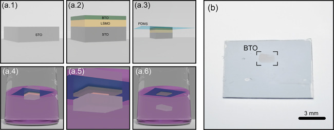
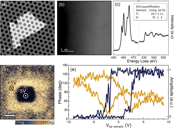
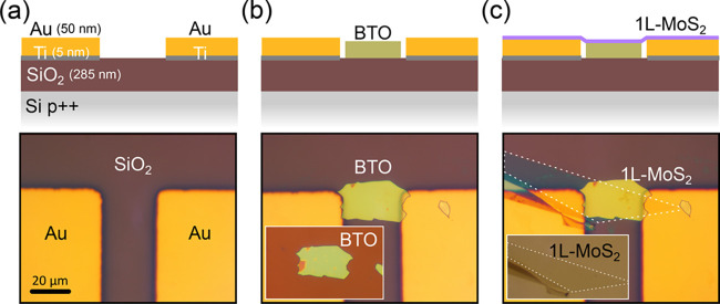
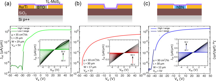
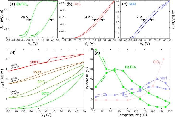
We demonstrate the fabrication of field-effect transistors based on single-layer MoS2 and a thin layer of BaTiO3 (BTO) dielectric, isolated from its parent epitaxial template substrate. Thin BTO provides an ultrahigh-κ gate dielectric effectively screening Coulomb scattering centers. These devices show mobilities substantially larger than those obtained with standard SiO2 dielectrics and comparable with values obtained with hexagonal boron nitride, a dielectric employed for fabrication of high-performance two-dimensional (2D) based devices. Moreover, the ferroelectric character of BTO induces a robust hysteresis of the current vs gate voltage characteristics, attributed to its polarization switching. This hysteresis is strongly suppressed when the device is warmed up above the tetragonal-to-cubic transition temperature of BTO that leads to a ferroelectric-to-paraelectric transition. This hysteretic behavior is attractive for applications in memory storage devices. Our results open the door to the integration of a large family of complex oxides exhibiting strongly correlated physics in 2D-based devices.

Keywords: barium titanate (BaTiO3); ferroelectric field effect transistor; ferroelectric perovskite oxide; freestanding complex oxide; molybdenum disulfide (MoS2).


Conflict of interest statement

The authors declare no competing financial interest.

Figures

Figure 1
Figure 1
Isolation of freestanding BTO thin films. (a) Steps for the isolation of freestanding BTO films. A thin film of LSMO (15 nm) is epitaxially grown onto a STO substrate and subsequently a 15–50 nm BTO film is epitaxially grown on top. Then a Gel-Film substrate is adhered to the BTO surface and the stack is immersed in an etching solution (0.5 mL HCl (37%), 0.5 mL KI (3M), 10 mL H2O) that attacks selectively the LSMO and releases the BTO film. (b) Picture of a Gel-Film carrier substrate with a macroscopic film of BTO (25 nm thick) on its surface.
Figure 2
Figure 2
Structural, chemical, and ferroelectric characterization of freestanding BTO thin films. (a) Z-contrast scanning transmission electron microscopy (STEM) low-magnification image of a 30 nm freestanding BTO flake transferred over a holey Si3N4 membrane. (b) Atomic resolution image showing the atomically sharp edge of the BTO flake viewed along the [001] direction. (c) Electron energy loss spectra of the TiL2,3 and OK edges acquired over the freestanding BTO flake. (d) PFM phase image on a 40 nm thick BTO flake after ferroelectric domain engineering by pooling a box-in-box pattern with tip voltages of +5 V and −5 V. (e) Local PFM amplitude (orange) and phase (black) hysteresis curves acquired on the transferred BTO flake.
Figure 3
Figure 3
Fabrication of field-effect devices integrating single-layer MoS2 channels and a BTO dielectric. The bottom panels show optical microscopy images at different steps of the fabrication. The top panels show a cartoon with the cross section of the corresponding optical microscopy images to further clarify the geometry of the devices. (a) Two prepatterned gold electrodes onto a SiO2/Si substrate. (b) A 50 nm BTO flake is picked up from a carrier SiO2/Si substrate (inset in bottom panel) and transferred in between the gold pads. (c) A single-layer MoS2 flake is transferred from a Gel-Film carrier substrate (see inset in bottom panel) onto the BTO flake and bridging the two prepatterned gold electrodes.
Figure 4
Figure 4
Gate tunable characteristics of 1L-MoS2 field-effect devices using BTO, SiO2 and hBN dielectrics. (a) Source drain current as a function of the gate voltage for a device integrating a BTO (48 nm)/SiO2 (285 nm) dielectric (see cartoon on top). (inset) Current vs drain-source bias voltage curves acquired at different gate voltages. (b) and (c) Similar data sets to (a) but collected for devices using a SiO2 (285 nm) dielectric layer and a hBN (∼30 nm)/SiO2 (285 nm) dielectric layer (see cartoons on top).
Figure 5
Figure 5
Characterization of the ferroelectric nature of the BTO dielectric. (a) to (c) Comparison between the hysteresis measured in the current vs gate voltage curves for BTO (48 nm)/SiO2 (285 nm) dielectric (a), SiO2 (285 nm) dielectric (b) and hBN (∼30 nm)/SiO2 (285 nm) dielectric (c). (d) Dependence of the current vs gate voltage curves as a function of the temperature. (e) Hysteresis of the current vs gate voltage curves as a function of the temperature for BTO, hBN, and SiO2 based devices.

References

    1. Dean C. R.; Young A. F.; Meric I.; Lee C.; Wang L.; Sorgenfrei S.; Watanabe K.; Taniguchi T.; Kim P.; Shepard K. L.; Hone J. Boron Nitride Substrates for High-Quality Graphene Electronics. Nat. Nanotechnol. 2010, 5 (10), 722–726. 10.1038/nnano.2010.172. - DOI - PubMed
    1. Frisenda R.; Navarro-Moratalla E.; Gant P.; Pérez De Lara D.; Jarillo-Herrero P.; Gorbachev R. V.; Castellanos-Gomez A. Recent Progress in the Assembly of Nanodevices and van Der Waals Heterostructures by Deterministic Placement of 2D Materials. Chem. Soc. Rev. 2018, 47 (1), 53.10.1039/C7CS00556C. - DOI - PubMed
    1. Ryu Y. K.; Frisenda R.; Castellanos-Gomez A. Superlattices Based on van Der Waals 2D Materials. Chem. Commun. 2019, 55 (77), 11498.10.1039/C9CC04919C. - DOI - PubMed
    1. Joyce B. A. Molecular Beam Epitaxy. Rep. Prog. Phys. 1985, 48 (12), 1637–1697. 10.1088/0034-4885/48/12/002. - DOI
    1. Novoselov K. S.; Mishchenko A.; Carvalho A.; Castro Neto A. H. 2D Materials and van Der Waals Heterostructures. Science 2016, 353 (6298), aac943910.1126/science.aac9439. - DOI - PubMed