. 2022 Sep 28;22(18):7690-7698.
doi: 10.1021/acs.nanolett.2c03169. Epub 2022 Sep 19.

Reconfigurable Compute-In-Memory on Field-Programmable Ferroelectric Diodes

Affiliations

Reconfigurable Compute-In-Memory on Field-Programmable Ferroelectric Diodes

Xiwen Liu et al. Nano Lett. .

Abstract

The deluge of sensors and data generating devices has driven a paradigm shift in modern computing from arithmetic-logic centric to data-centric processing. Data-centric processing require innovations at the device level to enable novel compute-in-memory (CIM) operations. A key challenge in the construction of CIM architectures is the conflicting trade-off between the performance and their flexibility for various essential data operations. Here, we present a transistor-free CIM architecture that permits storage, search, and neural network operations on sub-50 nm thick Aluminum Scandium Nitride ferroelectric diodes (FeDs). Our circuit designs and devices can be directly integrated on top of Silicon microprocessors in a scalable process. By leveraging the field-programmability, nonvolatility, and nonlinearity of FeDs, search operations are demonstrated with a cell footprint <0.12 μm2 when projected onto 45 nm node technology. We further demonstrate neural network operations with 4-bit operation using FeDs. Our results highlight FeDs as candidates for efficient and multifunctional CIM platforms.

Keywords: Compute in memory; ferroelectric diode; neural network; nonvolatile; parallel search; reconfigurable architecture; ternary content-addressable memory.


Conflict of interest statement

The authors declare the following competing financial interest(s): D.J., X.L., R.O., and E.A.S. have a provisional patent filed based on this work. The authors declare no other competing interests.

Figures

Figure 1
Figure 1
Reconfigurable CIM on Field-Programmable Ferroelectric Diodes. (a) Schematic diagram of FeD devices in a cross-bar structure with up and down polarization of the ferroelectric AlScN. The field programmability, nonvolatility, and nonlinearity of these devices can be leveraged for multiple, primitive data operations such as storage, search, and neural networks without the need for additional transistors, as shown in (b)–(d). (b) The two-terminal FeD devices show a diode-like self-rectifying behavior with nonlinearity >106 concurrently with an ON/OFF ratio over 102 and write-endurance over 104 cycles, making FeD devices well placed in the memory hierarchy for storage. Due to the high coercive field of AlScN, the read-disturbance would also be minimized which will result in high read-endurance. In addition, the high nonlinearity can suppress sneak currents without the need for additional access transistors, or selectors. (c) For search operations, a nonvolatile TCAM can be built upon 0-transistor/2-FeD cells, which serves as a building block in hardware implementation of in-memory computing for parallel search in big data applications. (d) For neural networks, FeD devices can provide programmability to distinct multiple conductive states with a high degree of linearity with respect to a number of electrical pulses. This allows mapping the matrix multiplication operation, a key kernel in neural-network computation, into reading the accumulated currents at each bitline of a FeD device by encoding an input vector into analog voltage amplitudes, and the matrix elements into conductances of an array of FeD devices. The matrix multiplication operation is benchmarked by mapping neural network weights to experimental FeD conductance states in a convolutional neural network architecture for both inference and the in situ learning task, and shows that our accuracies approach ideal software-level simulation on the MNIST data set.
Figure 2
Figure 2
Room-temperature electrical characterization of AlScN FeDs. (a) 3D schematic illustration of the AlScN FeD device and cross-sectional TEM image of the AlScN FeD, showing 45 nm AlScN as the ferroelectric switching layer. (b) The high-resolution phase-contrast TEM image obtained from the denoted regions (1) and (2) in (a) where the atomic structure of the ferroelectric and interface are visible. (c) PUND results of a 45 nm AlScN thin film with a pulse width of 400 ns and 2 μs delay between pulses. The PUND test reveals a saturated remanent polarization of 150 μC/cm2. (d) The extracted remanent polarizations from PUND measurements during the endurance test of AlScN films using 1.5 μs pulse width and 26 V amplitude. (e) 100 cycles of program and erase measurements over the 45 nm AlScN-based FeDs. (f) Distribution of HRS and LRS resistances during program and erase measurements in (e).
Figure 3
Figure 3
2-FeD TCAM cell for search operation. (a) A box schematic representation of a TCAM cell with match line (ML), search line (SL), and search line bar (SL bar) electrodes (left). Circuit diagrams of a single 16 transistor (16T) TCAM cell based on CMOS SRAM technology, and 2-transistor-2-resistor (2T2R) TCAMs based on resistive storage elements such as PCM and RRAM (center). The two FeD-based TCAM cell proposed in this work (right) significantly simplifies the TCAM design by using two FeDs connected in parallel but oppositely polarized. The cell structure makes it natural to utilize the FeD in crossbar memory arrays, in which the signal lines connecting to the anode and to the cathode are in parallel in a bit-search for the TCAM demonstration, as shown in Supplementary Figure S3. (b) Operation of a single TCAM cell comprising 2 FeDs for “match”, “mismatch”, and “do not care” (don't care) states. The full look up table of the two FeD-based TCAM cell is summarized in Supplementary Table 1. (c) Repeated, quasi-DC extraction of the resistance of the two FeDs TCAM cell for both match and mismatch states between the search data and the stored data bit ‘1’, showing a >100X difference over ML resistances. (d) Repeated quasi-DC measurement of the resistance of the two ferro-diodes TCAM cell for the stored data bit “Do not care”, using both query bit ‘1’ and ‘0’, which turns out that for both two queries the ML resistance of the two FeDs TCAM is high and thus no discharging through any of the two FeDs occurs. The sensing margin of our FeDs-based TCAM is a function of both the self-rectifying ratio and the ON/OFF conductance (or current) ratios. Per our detailed compact model (see Supplementary Note 1) the ON/OFF ratio of an FeD can be further improved by integrating a nonferroelectric insulator on top of the ferroelectric layer and engineering the thickness ratio between these ferroelectric and nonferroelectric insulator layers as well as the coercive field of the ferroelectric layer. Future studies will focus on further improving the sense margins by engineering these variables. (e) A benchmark comparison chart of lateral footprint of TCAM cells in various memory technologies:,− resistive random-access memories (RRAMs),, magnetic tunnel junction (MTJ) RAMs, floating gate transistor memory (FLASH), phase change memories (PCMs), and ferroelectric field-effect-transistor (FeFET). A single FeD area of 0.0081 μm2 is obtained for this estimate. The superior performance of our two FeD-based TCAM when compared to CMOS SRAM and other transistor plus-NVM devices-based architectures is evident.
Figure 4
Figure 4
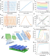
FeD-based neural network. (a) Gradual switching in FeD device by stepwise voltage modulation pulses. The FeD device showed superior linearity over 16 distinct states. Callout window (right panel) shows one cycle of gradual programming followed by an erase operation. (b) The FeD is demonstrated to be capable of voltage pulse-induced analog bipolar switching (left). Callout window (right) shows one cycle of gradual programming and gradual erasing. We note that the range of conductance in FeD devices used to program these states (∼25–250 nS) is much smaller as compared to the range of conductance used for TCAM operations (∼2–250 nS). This is primarily because this linearity in operation is better achieved in a smaller range of conductance. Further, the DNN inference application does not necessarily require a high range of conductance modulation.,, (c) Resistance retentions for 16 distinct resistance states. (d) Resistance states distribution of five separate FeDs subjected to sequences of 16 program pulses (2 μs pulse width) with interleaved reads (8 V). (e) Illustration of a CNN (including two convolutional layer and one fully connected layer) trained and weight mapping for the MNIST data set. As the hardware implementation of a neural network using FeD arrays can operate in a fully analog domain, the peripheral analog-to-digital converters could be waived. (f) Simulated performance of inference efficacy of the network in (e). In inference phase predictions are made by the quantized CNN over the MNIST test data set and inference accuracy is extracted. The simulations in (f) demonstrate that degradation of the network’s inference accuracy is less than 1% for low weight precision of just 3 bits for A < 0.5. (g) Simulations of in situ training of the network in (e) directly with the FeD devices implementing analog weight layers. Leveraged by the superior linearity in the gradual programming of the FeDs, the analog weight layers with 16 resistance states have been simulated to perform at a training accuracy comparable to the software baseline on floating-point numbers. This accuracy loss can be further reduced with more advanced low-precision training techniques and model compression techniques on software.

References

    1. LeCun Y.; Bengio Y.; Hinton G. Deep learning. nature 2015, 521 (7553), 436–444. 10.1038/nature14539. - DOI - PubMed
    1. Krizhevsky A.; Sutskever I.; Hinton G. E. Imagenet classification with deep convolutional neural networks. Communications of the ACM 2017, 60 (6), 84–90. 10.1145/3065386. - DOI
    1. He K.; Zhang X.; Ren S.; Sun J. In Deep residual learning for image recognition, Proceedings of the IEEE conference on computer vision and pattern recognition, 2016; pp 770–778.
    1. Sze V.; Chen Y.-H.; Yang T.-J.; Emer J. S. Efficient processing of deep neural networks: A tutorial and survey. Proceedings of the IEEE 2017, 105 (12), 2295–2329. 10.1109/JPROC.2017.2761740. - DOI
    1. Chen Y.-H.; Krishna T.; Emer J. S.; Sze V. Eyeriss: An energy-efficient reconfigurable accelerator for deep convolutional neural networks. IEEE journal of solid-state circuits 2017, 52 (1), 127–138. 10.1109/JSSC.2016.2616357. - DOI

Publication types

LinkOut - more resources