

Physical mechanisms involved in the formation and operation of memory devices based on a monolayer of gold nanoparticle-polythiophene hybrid materials
- PMID: 36132737
- PMCID: PMC9417853
- DOI: 10.1039/c9na00285e
Physical mechanisms involved in the formation and operation of memory devices based on a monolayer of gold nanoparticle-polythiophene hybrid materials
Abstract
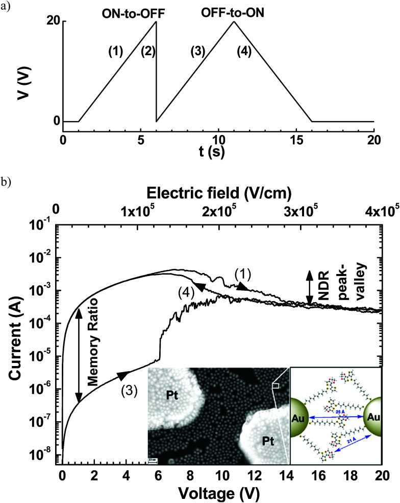
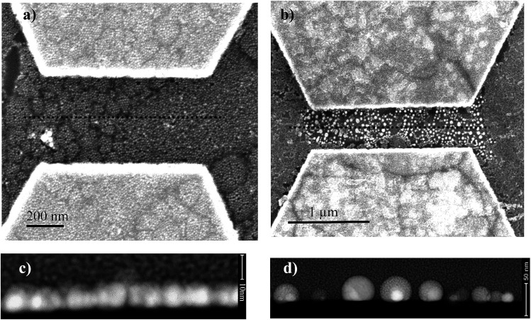
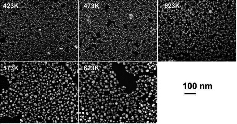
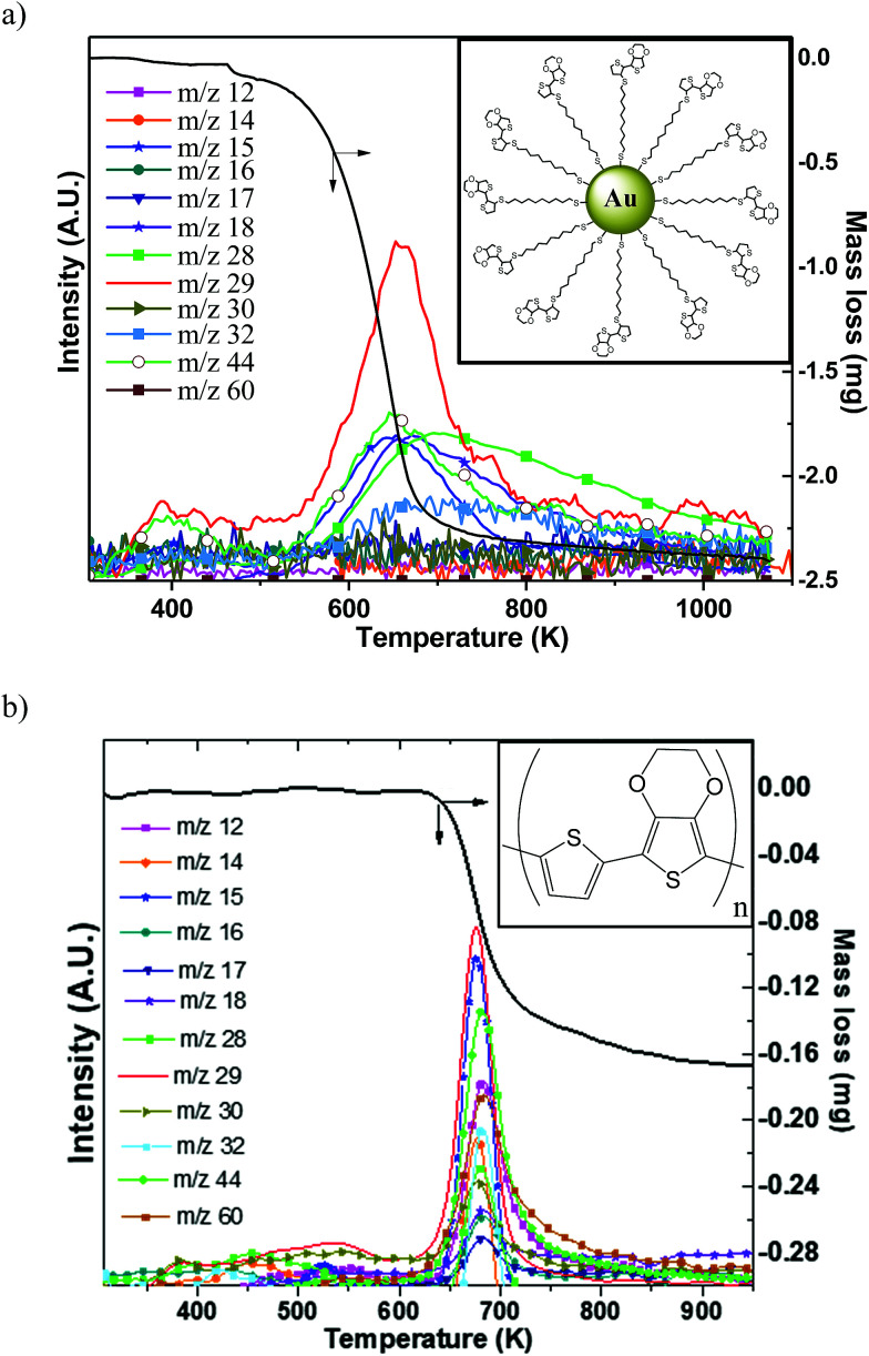
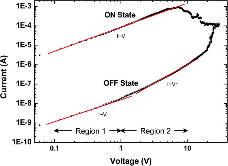
Understanding the physical and chemical mechanisms occurring during the forming process and operation of an organic resistive memory device is a requisite for better performance. Various mechanisms were suggested in vertically stacked memory structures, but the analysis remains indirect and needs destructive characterization (e.g. analysis of the cross-section to access the organic layers sandwiched between electrodes). Here, we report a study on a planar, monolayer thick, hybrid nanoparticle/molecule device (10 nm gold nanoparticles embedded in an electro-generated poly(2-thienyl-3,4-(ethylenedioxy)thiophene) layer), combining in situ physical (scanning electron microscopy, physicochemical thermogravimetry and mass spectroscopy, and Raman spectroscopy) and electrical (temperature dependent current-voltage) characterization on the same device. We demonstrate that the forming process causes an increase in the gold particle size, almost 4 times larger than the starting nanoparticles, and that the organic layer undergoes a significant chemical rearrangement from an sp3 to sp2 amorphous carbon material. Temperature dependent electrical characterization of this nonvolatile memory confirms that the charge transport mechanism in the device is consistent with a trap-filled space charge limited current in the off state, with the sp2 amorphous carbon material containing many electrically active defects.
This journal is © The Royal Society of Chemistry.
Conflict of interest statement
There are no conflicts to declare.
Figures


References
-
- Pan F. Gao S. Chen C. Song C. Zeng F. Recent progress in resistive random access memories: materials, switching mechanisms, and performance. Mater. Sci. Eng., R. 2014;83:1–59. doi: 10.1016/j.mser.2014.06.002. - DOI
-
- Zhang T. Guérin D. Alibart F. Vuillaume D. Lmimouni K. Lenfant S. Yassin A. Oçafrain M. Blanchard P. Roncali J. Negative Differential Resistance, Memory, and Reconfigurable Logic Functions Based on Monolayer Devices Derived from Gold Nanoparticles Functionalized with Electropolymerizable TEDOT Units. J. Phys. Chem. C. 2017;121(18):10131–10139. doi: 10.1021/acs.jpcc.7b00056. - DOI
-
- Yassin A. Ocafrain M. Blanchard P. Mallet R. Roncali J. Synthesis of Hybrid Electroactive Materials by Low-Potential Electropolymerization of Gold Nanoparticles Capped with Tailored EDOT-Thiophene Precursor Units. ChemElectroChem. 2014;1(8):1312–1318. doi: 10.1002/celc.201402087. - DOI
-
- Ma L. Liu J. Yang Y. Organic electrical bistable devices and rewritable memory cells. Appl. Phys. Lett. 2002;80(16):2997–2999. doi: 10.1063/1.1473234. - DOI
LinkOut - more resources
Full Text Sources