

Femtosecond laser-induced non-thermal welding for a single Cu nanowire glucose sensor
- PMID: 36133038
- PMCID: PMC9419468
- DOI: 10.1039/c9na00740g
Femtosecond laser-induced non-thermal welding for a single Cu nanowire glucose sensor
Abstract
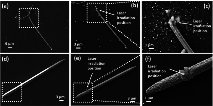
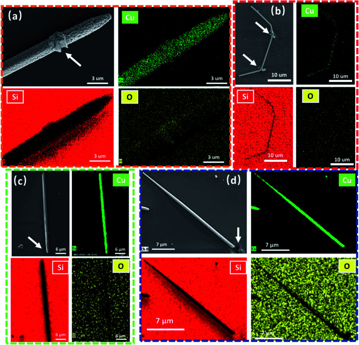
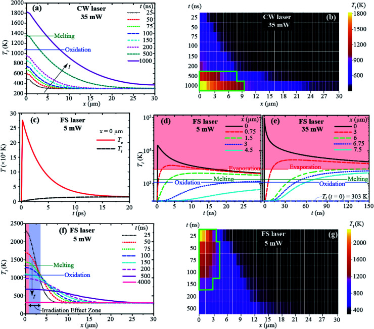
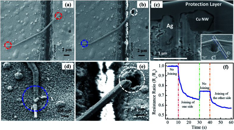
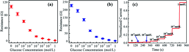
Copper nanowires (CuNWs) are a key building block to facilitate carrier conduction across a broad range of nanodevices. For integration into nanoscale devices, manipulation and welding of these nanowires need to be overcome. Based on high energy density laser processing investigation, we report on innovative welding of single CuNWs to a silver film using a tightly focused laser beam combined with manipulation of CuNWs through the dielectrophoresis (DEP) method. Two types of lasers, femtosecond (FS) and continuous-wave (CW), were employed to analyze, improve, and control Cu-NW melting characteristics under high energy density irradiation. The FS laser welding of CuNWs resulted in a metallic joint with a low contact resistance suitable for functional electronic nanodevices. Computational simulations using the 1-D heat diffusion equation and finite difference method (FDM) were performed to gain an insight into metal-laser interactions for high performance welded contact development. Simulation studies on lasers established contrasting melting behavior of metal under laser irradiation. The device feasibility of CuNW based welded contacts was evaluated in terms of the electrical performance of a glucose sensor. It was possible to sense glucose concentration down to 10-6 M, demonstrating a path towards integration of CuNWs into wearable, flexible nanoelectronic devices.
This journal is © The Royal Society of Chemistry.
Conflict of interest statement
We have no conflicts of interest to declare.
Figures
Similar articles
-
Enhancement of the Conductivity and Uniformity of Silver Nanowire Flexible Transparent Conductive Films by Femtosecond Laser-Induced Nanowelding.Nanomaterials (Basel). 2019 May 1;9(5):673. doi: 10.3390/nano9050673. Nanomaterials (Basel). 2019. PMID: 31052377 Free PMC article.
-
Laser-Induced Self-Limiting Welding of Ag Nanowires with High Mechanical and Electrical Performance.Adv Mater. 2024 Nov;36(48):e2408575. doi: 10.1002/adma.202408575. Epub 2024 Oct 14. Adv Mater. 2024. PMID: 39400396
-
Efficient metallic nanowire welding using the Eddy current method.Nanotechnology. 2019 Feb 8;30(6):065708. doi: 10.1088/1361-6528/aaf13d. Nanotechnology. 2019. PMID: 30524023
-
A Review: Laser Welding of Dissimilar Materials (Al/Fe, Al/Ti, Al/Cu)-Methods and Techniques, Microstructure and Properties.Materials (Basel). 2021 Dec 24;15(1):122. doi: 10.3390/ma15010122. Materials (Basel). 2021. PMID: 35009268 Free PMC article. Review.
-
Advancements in Copper Nanowires: Synthesis, Purification, Assemblies, Surface Modification, and Applications.Small. 2018 Jun;14(26):e1800047. doi: 10.1002/smll.201800047. Epub 2018 Apr 30. Small. 2018. PMID: 29707894 Review.
Cited by
-
Thermal Nonlinear Klein-Gordon Equation for Nano-/Micro-Sized Metallic Particle-Attosecond Laser Pulse Interaction.Materials (Basel). 2021 Feb 10;14(4):857. doi: 10.3390/ma14040857. Materials (Basel). 2021. PMID: 33579005 Free PMC article.
-
Femtosecond Laser Direct Writing of Flexible Electronic Devices: A Mini Review.Materials (Basel). 2024 Jan 24;17(3):557. doi: 10.3390/ma17030557. Materials (Basel). 2024. PMID: 38591371 Free PMC article. Review.
-
Femtosecond Laser-Induced Nano-Joining of Volatile Tellurium Nanotube Memristor.Nanomaterials (Basel). 2023 Feb 21;13(5):789. doi: 10.3390/nano13050789. Nanomaterials (Basel). 2023. PMID: 36903667 Free PMC article.
-
Synthesis and Unique Behaviors of High-Purity HEA Nanoparticles Using Femtosecond Laser Ablation.Nanomaterials (Basel). 2024 Mar 21;14(6):554. doi: 10.3390/nano14060554. Nanomaterials (Basel). 2024. PMID: 38535702 Free PMC article.
-
Multiphoton Absorption Simulation of Sapphire Substrate under the Action of Femtosecond Laser for Larger Density of Pattern-Related Process Windows.Micromachines (Basel). 2021 Dec 17;12(12):1571. doi: 10.3390/mi12121571. Micromachines (Basel). 2021. PMID: 34945421 Free PMC article.
References
-
- Falk A. L. Koppens F. H. Chun L. Y. Kang K. de Leon Snapp N. Akimov A. V. Jo M.-H. Lukin M. D. Park H. Nat. Phys. 2009;5:475.
-
- NormanáZhou Y. J. Mater. Chem. 2012;22:12997. doi: 10.1039/C2JM31979A. - DOI
LinkOut - more resources
Full Text Sources