. 2020 Jan 23;2(2):869-877.
doi: 10.1039/c9na00762h. eCollection 2020 Feb 18.

Ultrathin sputter-deposited plasmonic silver nanostructures

Affiliations

Ultrathin sputter-deposited plasmonic silver nanostructures

Selina Goetz et al. Nanoscale Adv. .

Abstract

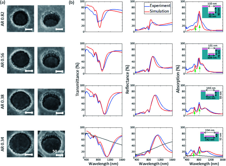
In this study, ultrathin silver plasmonic nanostructures are fabricated by sputter deposition on substrates patterned by nanoimprint lithography, without additional lift-off processes. Detailed investigation of silver growth on different substrates results in a structured, defect-free silver film with thickness down to 6 nm, deposited on a thin layer of doped zinc oxide. Variation of the aspect ratio of the nanostructure reduces grain formation at the flanks, allowing for well-separated disk and hole arrays, even though conventional magnetron sputtering is less directional than evaporation. The resulting disk-hole array features high average transmittance in the visible range of 71% and a strong plasmonic dipole resonance in the near-infrared region. It is shown that the ultrathin Ag film exhibits even lower optical losses in the NIR range compared to known bulk optical properties. The presented FDTD simulations agree well with experimental spectra and show that for defect-free, ultrathin Ag nanostructures, bulk optical properties of Ag are sufficient for a reliable simulation-based design.


Conflict of interest statement

There are no conflicts to declare.

Figures

Fig. 1
Fig. 1. SEM characterization of ultrathin sputter deposited Ag films with increasing thickness (4 nm, 6 nm and 8 nm) on different substrate materials. The investigated substrates are bare glass, NIL-resist (OrmoStamp) and 10 nm AZO on glass, respectively. The scale bar is 200 nm in all SEM images.
Fig. 2
Fig. 2. (a) Experimental and simulated (Sim.) transmittance and reflectance spectra of 6 nm Ag on 10 nm AZO. Simulations are performed for continuous layers with different literature values of bulk Ag. (b) Real and imaginary part of complex permittivity of 6 nm Ag derived from the experiment and values from the literature.
Fig. 3
Fig. 3. (a) Schematic of the nanostructure under investigation. (b) SEM images (at 30°-tilted view) for different Ag thicknesses on 10 nm AZO deposited on a nanostructured resist (height 90 nm, period 200 nm and diameter app. 100 nm). The evolution of grain growth on the sidewalls during sputter deposition can be observed. The scalebar is the same for all images.
Fig. 4
Fig. 4. (a) SEM images at normal and 30° tilted view for different aspect ratios (ARs) of the disk–hole array with 10 nm AZO and 6 nm Ag. (b) Experimental (blue) and FDTD-simulated (red) transmittance, reflectance and absorption spectra of the corresponding structures. Geometry parameters used for the simulations are indicated by the schematic insets. The grey solid line in the last row represents the experimental spectra of the planar structure with same layer thicknesses.
Fig. 5
Fig. 5. Simulated transmittance spectra and surface charge density at resonance positions for the periodic (a–c) disk array, (d–f) hole array and (g) disk–hole array for a variety of geometrical parameters (given in the insets). An offset has been introduced in the transmittance parameter variations for better distinction. Scale of charge density is adapted for every resonance. Angle wavelength map for the disk–hole array (with same parameters as in (g)) for (h) TE-polarization and (i) TM Polarization. Resonance positions are indicated by dashed lines. All simulations are done for resist height 55 nm, AZO thickness of 10 nm and Ag thickness of 6 nm.

References

    1. Zilberberg K. Riedl T. J. Mater. Chem. A. 2016;4:14481–14508. doi: 10.1039/C6TA05286J. - DOI
    1. West P. R. Ishii S. Naik G. V. Emani N. K. Shalaev V. M. Boltasseva A. Laser Photonics Rev. 2010;4:795–808. doi: 10.1002/lpor.200900055. - DOI
    1. Yang X. Gao P. Yang Z. Zhu J. Huang F. Ye J. Sci. Rep. 2017;7:44576. doi: 10.1038/srep44576. - DOI - PMC - PubMed
    1. Peng L. Liu D. Cheng H. Sol. Energy Mater. Sol. Cells. 2019;193:7–12. doi: 10.1016/j.solmat.2018.12.039. - DOI
    1. Ko R. H. H. Khalatpour A. Clark J. K. D. Kherani N. P. APL Mater. 2018;6:121112. doi: 10.1063/1.5052261. - DOI