. 2019 Jul 1;1(8):3119-3130.
doi: 10.1039/c9na00256a. eCollection 2019 Aug 6.

Non-ohmic behavior and resistive switching of Au cluster-assembled films beyond the percolation threshold

Affiliations

Non-ohmic behavior and resistive switching of Au cluster-assembled films beyond the percolation threshold

M Mirigliano et al. Nanoscale Adv. .

Abstract

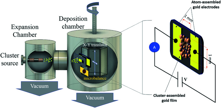
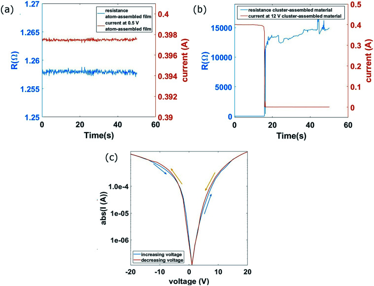
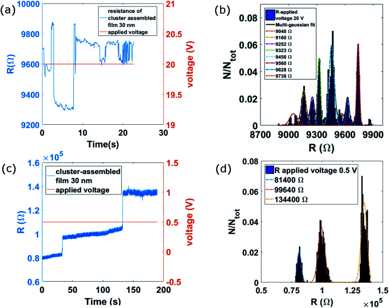
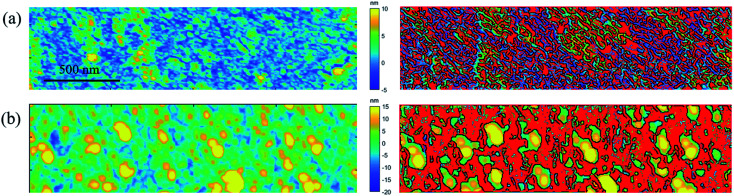
Networks based on nanoscale resistive switching junctions are considered promising for the fabrication of neuromorphic computing architectures. To date random networks of nanowires, nanoparticles, and metal clusters embedded in a polymeric matrix or passivated by shell of ligands or oxide layers have been used to produce resistive switching systems. The strategies applied to tailor resistive switching behavior are currently based on the careful control of the volume fraction of the nanoscale conducting phase that must be fixed close to the electrical percolation threshold. Here, by blending laboratory and computer experiments, we demonstrate that metallic nanostructured Au films fabricated by bare gold nanoparticles produced in the gas phase and with thickness well beyond the electrical percolation threshold, show a non-ohmic electrical behavior and complex and reproducible resistive switching. We observe that the nanogranular structure of the Au films does not evolve with thickness: this introduces a huge number of defects and junctions affecting the electrical transport and causing a dynamic evolution of the nanoscale electrical contacts under the current flow. To uncover the origin of the resistive switching behavior in Au cluster-assembled films, we developed a simple computational model for determining the evolution of a model granular film under bias conditions. The model exploits the information provided by experimental investigation about the nanoscale granular morphology of real films. Our results show that metallic nanogranular materials have functional properties radically different from their bulk counterparts, in particular nanostructured Au films can be fabricated by assembling bare gold clusters which retain their individuality to produce an all-metal resistive switching system.


Conflict of interest statement

There are no conflicts to declare.

Figures

Scheme 1
Scheme 1. Schematic representation (not to scale) of the apparatus for the deposition of cluster-assembled Au films. It consists of a pulsed microplasma cluster source mounted on the axis of differentially pumped vacuum chambers, the PMCS produces a supersonic expansion of an inert gas seeded with metallic clusters to form a cluster beam. The beam is intercepted by a substrate placed on a mobile holder (manipulator) in the deposition chamber. Substrates with gold electrodes previously deposited by thermal evaporation are mounted on the sample holder. A quartz microbalance attached to the manipulator is periodically exposed to the cluster beam to monitor the amount of deposited material. In situ electrical characterization during the cluster-assembled film growth is performed.
Fig. 1
Fig. 1. Top: percolation curves of an atomic-assembled gold film (blue) and of a cluster-assembled film (red), with the conductance (the inverse of the measured film resistance) on the y-axis in logarithmic scale and the film thickness on the x-axis; bottom: SEM images of the film morphology are associated to different film thicknesses and electrical behaviour. (A) continuous atom-assembled film (scale bar 200 nm). (B–D): Images of the principal steps of growth of a cluster-assembled metallic films are reported: (B) insulating stage; (C) close to percolation; (D) conducting regime: a fully connected thick-film (scale bar 100 nm).
Fig. 2
Fig. 2. From left to right: (a) histogram in logarithmic scale of the height of the clusters measured by AFM on the smallest coverage sample. (b) relative island heights (measured by AFM) and the relative radius (measured from SEM micrographs, see Materials and methods) as a function of the coverage (the subscript ‘0’ refer to the smallest coverage sample). (c) histogram of the equivalent radius of the grains obtained segmenting a SEM micrograph of the thick film, in logarithmic scale.
Fig. 3
Fig. 3. (a) electrical resistance and current of an atom-assembled Au film 100 nm thick as a function of time under the application of 0.5 V. (b) electrical resistance and current of a cluster-assembled Au film 65 nm thick as a function of time under the application of 12 V in the proximity of the forming step; the current is approximately equal to that circulating in the atom-assembled film (c) IV curve of a cluster-assembled film after the activation of the switching activity in semilog-y scale.
Fig. 4
Fig. 4. (a) electrical resistance of a cluster-assembled film with thickness 30 nm under the bias of 20 V; several switch events in the interval time of 20 s are evident. (b) Histogram of the resistance values assumed by the sample under the application of 20 V in a time window of 200 s. (c) Electrical resistance of the same sample under the bias of 0.5 V. (d) Histogram of the resistance values assumed by the sample under the application of 0.5 V in a time window of 200 s.
Fig. 5
Fig. 5. Topographical AFM images of different Au films (left column) with the matching current map superimposed to the topographical one (right column), where the red regions are the conductive one. (a) Atom-assembled Au film. (b) Cluster-assembled Au film 37 nm thick.
Fig. 6
Fig. 6. (a) Percolation curve of conductance as a function of the coverage value. In the inset, images of some structural configurations are depicted. (b) Resistance as a function of simulation steps in a system of 50 × 70 pixels; the resistance values at the time steps corresponding to the shown configurations are highlighted. (c–f) The structure (c) and the maps of electrostatic potential (d), current (e) and dissipated power (f) in a system of 50 × 70 pixels, (coverage = 0.64). Values at three unlike microstructure arrangements are shown. Modifications in the structural parameters determine the continuous creation and destruction of percolative paths.
Fig. 7
Fig. 7. (a) Top: the resistance as function of simulation steps (the same data as in Fig. 6b) normalized to the initial resistance of a system 50 × 70 pixels; bottom: resistance evolution normalized to the initial resistance of the cluster-assembled film under a bias of 5 V as function of time. (b) The histogram of the resistance values both for the cluster-assembled film and the simulation.

References

    1. Zidan M. A. Strachan J. P. Lu W. D. Nat. Electron. 2018;1:22–29. doi: 10.1038/s41928-017-0006-8. - DOI
    1. Nawrocki R. A. Voyles R. M. Shaheen S. E. IEEE Trans. Electron Devices. 2016;63:3819–3829.
    1. Avizienis A. V. Sillin H. O. Martin-Olmos C. Shieh H. Aono M. Stieg A. Z. et al. . PLoS One. 2012;7:1–8. doi: 10.1371/journal.pone.0042772. - DOI - PMC - PubMed
    1. Ohno T. Hasegawa T. Tsuruoka T. Terabe K. Gimzewski J. K. Aono M. Nat. Mater. 2011;10:591–595. doi: 10.1038/nmat3054. - DOI - PubMed
    1. Bose S. K. Shirai S. Mallinson J. B. Brown S. A. Faraday Discuss. 2019;213:471. doi: 10.1039/C8FD00109J. - DOI - PubMed