. 2020 Jun 9;2(8):3156-3163.
doi: 10.1039/d0na00046a. eCollection 2020 Aug 11.

Flexible transparent graphene laminates via direct lamination of graphene onto polyethylene naphthalate substrates

Affiliations

Flexible transparent graphene laminates via direct lamination of graphene onto polyethylene naphthalate substrates

Ismael G Serrano et al. Nanoscale Adv. .

Abstract

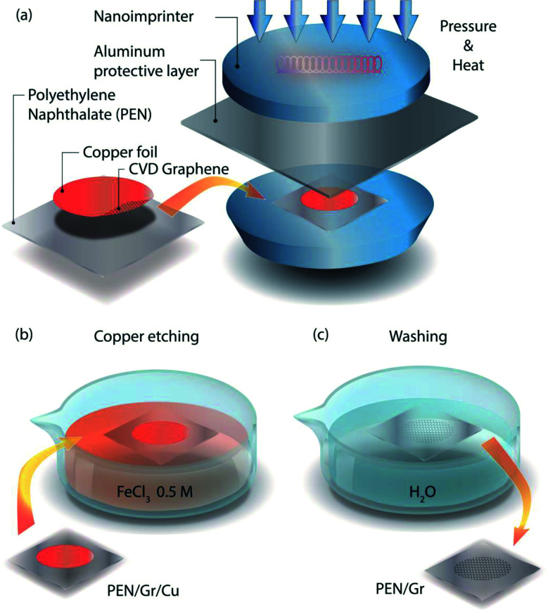
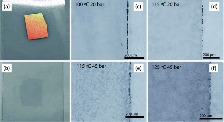
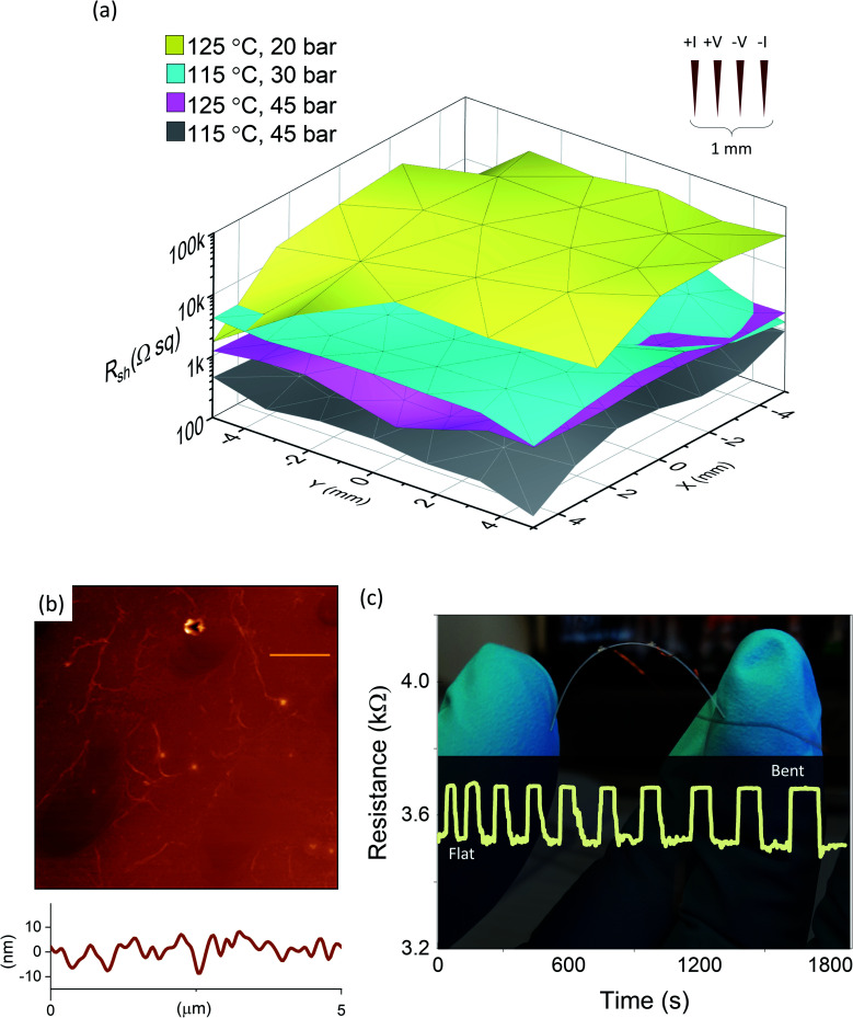
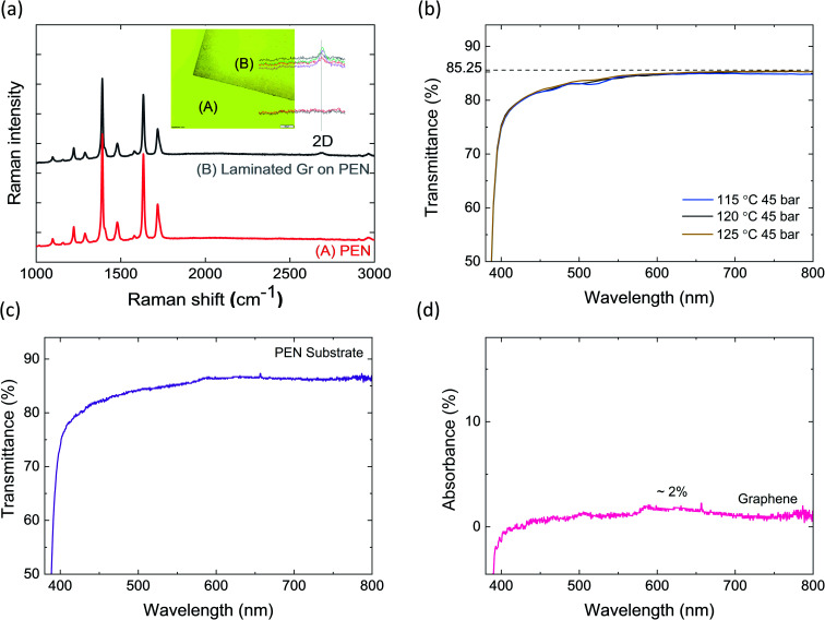
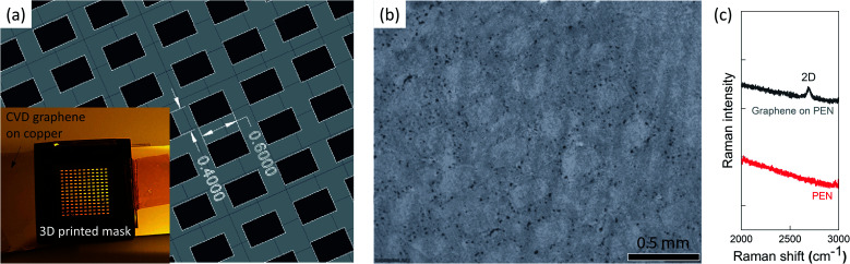
Graphene, with its excellent electrical, mechanical, and optical properties, has emerged as an exceptional material for flexible and transparent nanoelectronics. Such versatility makes it compelling to find new pathways to lay graphene sheets onto smooth, flexible substrates to create large-scale flexible transparent graphene conductors. Here, we report the realization of flexible transparent graphene laminates by direct adhesion of chemical vapor deposition (CVD) graphene on a polyethylene naphthalate (PEN) substrate, which is an emerging standard for flexible electronics. By systematically optimizing the conditions of a hot-press technique, we have identified that applying optimum temperature and pressure can make graphene directly adhere to flexible PEN substrates without any intermediate layer. The resultant flexible graphene films are transparent, have a standard sheet resistance of 1 kΩ with high bending resilience, and high optical transmittance of 85%. Our direct hot-press method is achieved below the glass transition temperature of the PEN substrate. Furthermore, we demonstrate press-assisted embossing for patterned transfer of graphene, and hence it can serve as a reliable new means for creating universal, transparent conducting patterned films for designing flexible nanoelectronic and optoelectronic components.


Conflict of interest statement

There are no conflicts to declare.

Figures

Fig. 1
Fig. 1. (a) Schematic representation of the nanoimprint system and lamination process, (b) Cu etching process, and (c) DI water rinsing.
Fig. 2
Fig. 2. (a) PEN/Gr/Cu after lamination, (b) PEN/Gr after copper etching and rinsing. Optical microscope images of (c) sample 4 (100 °C, 20 bar), (d) sample 7 (115 °C, 20 bar), (e) sample 9 (115 °C, 45 bar), (f) sample 15 (125 °C, 45 bar).
Fig. 3
Fig. 3. (a) Sheet resistance map for laminated samples at 125 °C, 20 bar (yellow), 115 °C, 30 bar (cyan), 125 °C, 45 bar (pink), 115 °C, 45 bar (grey). (b) Atomic force microscope image of a laminated sample with a line profile over 5 μm (shown in the scale bar). (c) Bending measurements performed on a laminated sample showing measurements under normal and bent conditions.
Fig. 4
Fig. 4. (a) Raman spectra measured on a laminated area on several samples (B) and Raman spectra measured on PEN on the non-laminated area (A). The 2D peak of graphene is only visible in the laminated area (B). Inset shows the two different areas on a sample along with Raman peaks in several points in A and B regions. (b) Transmittance as a function of wavelength for different samples. 120 °C 45 bar (black), 115 °C 45 bar (blue), and 125 °C 45 bar (yellow) in the visible spectrum wavelength. (c) Transmittance as a function of wavelength for PEN substrate. (d) Absorbance of graphene laminated on the substrate obtained by deconvoluting substrate contribution (c) from total transmittance (b).
Fig. 5
Fig. 5. (a) Pattern of mask for 3D printing. Inset: 3D printed mask on initial CVD graphene containing copper foil. (b) Microscope image of the patterned graphene with a 3d printed mask. (c) Raman spectra of graphene region and bare PEN region after lamination.

References

    1. Novoselov K. S. Jiang D. Schedin F. Booth T. J. Khotkevich V. V. Morozov S. V. Geim A. K. Proc. Natl. Acad. Sci. U. S. A. 2005;102:10451. doi: 10.1073/pnas.0502848102. - DOI - PMC - PubMed
    1. Bonaccorso F. Sun Z. Hasan T. Ferrari A. C. Nat. Photonics. 2010;4:611. doi: 10.1038/nphoton.2010.186. - DOI
    1. Bae S. Kim H. Lee Y. Xu X. Park J.-S. Zheng Y. Balakrishnan J. Lei T. Ri Kim H. Il Song Y. Kim Y.-J. Kim K. S. Özyilmaz B. Ahn J.-H. Hong B. H. Iijima S. Nat. Nanotechnol. 2010;5:574. doi: 10.1038/nnano.2010.132. - DOI - PubMed
    1. Kim K. S. K. S. K. S. Zhao Y. Jang H. Lee S. Y. S. Y. Kim J. M. J. M. Ahn J. J.-H. J.-H. Kim P. Choi J.-Y. J.-Y. Hong B. H. B. H. Kim K. S. K. S. K. S. Ahn J. J.-H. J.-H. Kim P. Choi J.-Y. J.-Y. Hong B. H. B. H. Nature. 2009;457:706. doi: 10.1038/nature07719. - DOI - PubMed
    1. Serrano I. G. Panda J. Denoel F. Vallin Ö. Phuyal D. Karis O. Kamalakar M. V. Nano Lett. 2019;19:666. doi: 10.1021/acs.nanolett.8b03520. - DOI - PubMed