Growth and Characterization of Ultrathin Vanadium Oxide Films on HOPG
- PMID: 36144922
- PMCID: PMC9505911
- DOI: 10.3390/nano12183134
Growth and Characterization of Ultrathin Vanadium Oxide Films on HOPG
Abstract
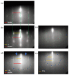
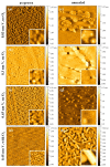
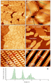
Integration of graphene into various electronic devices requires an ultrathin oxide layer on top of graphene. However, direct thin film growth of oxide on graphene is not evident because of the low surface energy of graphene promoting three-dimensional island growth. In this study, we demonstrate the growth of ultrathin vanadium oxide films on a highly oriented pyrolytic graphite (HOPG) surface, which mimics the graphene surface, using (oxygen-assisted) molecular beam epitaxy, followed by a post-annealing. The structural properties, surface morphology, and chemical composition of the films have been systematically investigated by in situ reflection high-energy electron diffraction during the growth and by ex situ techniques, such as atomic force microscopy, scanning tunneling microscopy, transmission electron microscopy, and X-ray photoelectron spectroscopy (XPS). Crystalline monolayer vanadium oxide can be achieved on HOPG by systematically tuning the deposition time of V atoms and by subsequent annealing at 450 °C in controlled atmospheres. Increasing the partial pressure of O2 during the deposition seems to decrease the mobility of V atoms on the graphitic surface of HOPG and promote the formation of a two-dimensional (2D) vanadium oxide. The obtained oxide layers are found to be polycrystalline with an average grain size of 15 nm and to have a mixed-valence state with mainly V5+ and V4+. Moreover, XPS valence band measurements indicate that the vanadium oxide is insulating. These results demonstrate that a 2D insulating vanadium oxide can be grown directly on HOPG and suggest vanadium oxide as a promising candidate for graphene/oxide heterostructures.
Keywords: 2D; HOPG; X-ray photoelectron spectroscopy; atomic force microscopy; molecular beam epitaxy; scanning tunneling microscopy; thin films; vanadium oxide.
Conflict of interest statement
The authors declare no conflict of interest. The funders had no role in the design of the study; in the collection, analyses, or interpretation of data; in the writing of the manuscript; or in the decision to publish the results.
Figures


References
-
- Dhinakaran V., Lavanya M., Vigneswari K., Ravichandran M., Vijayakumar M.D. Review on exploration of graphene in diverse applications and its future horizon. Mater. Today Proc. 2020;27:824–828. doi: 10.1016/j.matpr.2019.12.369. - DOI
Grants and funding
LinkOut - more resources
Full Text Sources

