Review
. 2022 Sep 10;12(18):3146.
doi: 10.3390/nano12183146.

Graphene-Induced Performance Enhancement of Batteries, Touch Screens, Transparent Memory, and Integrated Circuits: A Critical Review on a Decade of Developments

Affiliations
Review

Graphene-Induced Performance Enhancement of Batteries, Touch Screens, Transparent Memory, and Integrated Circuits: A Critical Review on a Decade of Developments

Joydip Sengupta et al. Nanomaterials (Basel). .

Abstract

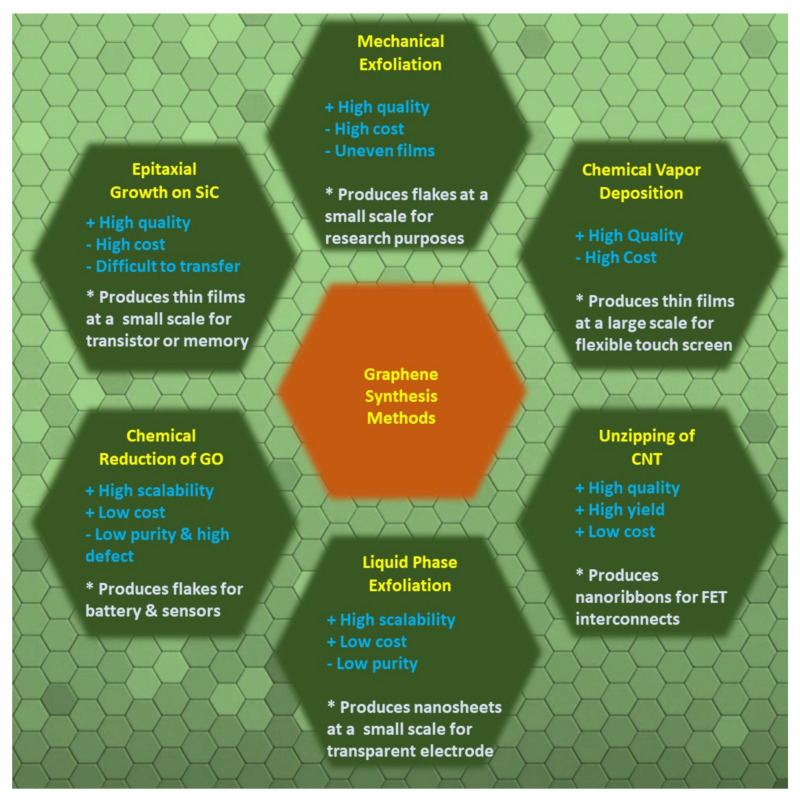
Graphene achieved a peerless level among nanomaterials in terms of its application in electronic devices, owing to its fascinating and novel properties. Its large surface area and high electrical conductivity combine to create high-power batteries. In addition, because of its high optical transmittance, low sheet resistance, and the possibility of transferring it onto plastic substrates, graphene is also employed as a replacement for indium tin oxide (ITO) in making electrodes for touch screens. Moreover, it was observed that graphene enhances the performance of transparent flexible electronic modules due to its higher mobility, minimal light absorbance, and superior mechanical properties. Graphene is even considered a potential substitute for the post-Si electronics era, where a high-performance graphene-based field-effect transistor (GFET) can be fabricated to detect the lethal SARS-CoV-2. Hence, graphene incorporation in electronic devices can facilitate immense device structure/performance advancements. In the light of the aforementioned facts, this review critically debates graphene as a prime candidate for the fabrication and performance enhancement of electronic devices, and its future applicability in various potential applications.

Keywords: field effect transistor; flexible electronics; graphene; nanomaterial; touch screen; transparent electronics.


Conflict of interest statement

The authors declare no conflict of interest.

Figures

Scheme 1
Scheme 1
Mapping of graphene properties with potential applications in electronic devices.
Figure 1
Figure 1
(Top left) STM topography reveals atomically resolved graphene lattice. The blue and green spheres indicate two carbon atoms of the unit cell, labelled A and B. (Reproduced with permission from ref [19]). (Top right) High-resolution images of graphene (the scale bar is 2 nm). Inset (A): the filtered image of the area within the red rectangular frame. Inset (B): pixel intensity profile of the graphene along the blue line in inset (A), which was used to calculate the distance between the second-nearest neighboring carbon atoms in the hexagonal carbon ring. Inset (C) Normal-incidence selected area electron diffraction pattern of graphene. (Reproduced with permission from ref [20]. (Bottom right) Graphene films with different thicknesses (a) 86 nm, (b) 22 nm, and (c) 14 nm. (Reproduced with permission from ref [21]. (Bottom left) Various graphene nanoribbons (GNRs): (a) zigzag GNR (ZGNR), (b) armchair GNR (AGNR), and (c) chiral GNR (CGNR). The numbers 1, 2, 3, … in (a,b) indicate the zigzag and armchair chains of the GNRs and their width. (Reproduced with permission from ref [22]).
Figure 2
Figure 2
(a) Brillouin zone of graphene with high-symmetry points K, Γ, and M. The reciprocal lattice vectors, K1 and K2, are in Cartesian coordinates. (b) Band structure of monolayer graphene along the Γ K M direction. (c) Surface plot and (d) contour plot of energy dispersion in graphene. Note that there are six K points where the bandgap becomes zero. (e) The shape of the valence and the conduction bands of graphene resembles cone-like structures called the “Dirac cone” that meet at the Dirac point. The band position can be shifted by electron or hole doping, thus the Fermi level (EF) is displaced to higher or lower energy, respectively, with reference to the Dirac point. (Reproduced with permission from refs [27,28,29].
Figure 3
Figure 3
Similar to a single layer, a pristine bi-layer has no band gap, but a gap can be created through proper doping (a) or electric field application (b). (Reproduced with permission from refs [32,33].
Figure 4
Figure 4
Classification of graphene-based materials. (Reproduced with permission from ref [34]).
Scheme 2
Scheme 2
Mapping of graphene growth methods, product quality, and target applications in electronic devices.
Figure 5
Figure 5
The charge/discharge intercalation mechanism of Li-ion battery. (Reproduced with permission from ref [48]).
Figure 6
Figure 6
(Left) Schematic structure of the binding conditions of Nitrogen (N) and Boron (B) in a graphene lattice, indicated by dotted magenta rings. (Right) Ragone plots for pristine graphene, N-doped graphene, B-doped graphene, graphene oxide (GO), and GO500-based cells with lithium metal as the counter/reference electrode. The calculation of gravimetric energy and power density was based on the active material mass of a single electrode. (Reproduced with permission from ref [56].
Figure 7
Figure 7
(Left) Schematic of Li deposited on graphene grown on Cu. Schematic of GCNT–Li formation. (Right above) Voltage vs. time of lithiation and delithiation processes of GCNT–Li. (Right below) SEM images of delithiated GCNT–Li (0.7 mAh cm−2 at 2 mA cm−2) after 250 cycles. (Reproduced with permission from ref [77].
Figure 8
Figure 8
Metal grid/graphene hybrid transparent electrode. The yellow lines in the figure represent the metal grid. The grid size and grid-line width in the figure are only illustrative and are not scaled with the graphene molecular structure. (Reproduced with permission from ref [112]).
Figure 9
Figure 9
Graphene-based touch sensor prototype. (a) Overlapped top and bottom PET panels with the spray-coated graphene row (Tx) and column (Rx) electrodes and conductive Ag pads. (b) Complete system (touch sensor + controller + computer) operated in multi-touch mode. (c) Complete touch sensor interfaced with external connections. (Reproduced with permission from ref [119]).
Figure 10
Figure 10
(Left) FTM can be utilized for transparent and flexible electronics that require integration of logic, memory, and display, on a single substrate with high transparency and endurance under stress. (Middle) Photograph of the large-scale transparent–flexible FTM array fabricated on PEN substrate. FTM cell is transparent enough to see objects through it without image distortion flex. (Right) Memory characteristics of FTM. (Reproduced with permission from ref [123]).
Figure 11
Figure 11
Schematic sketch of a GFET. (Reproduced with permission from ref [165].
Scheme 3
Scheme 3
The future path of graphene.

References

    1. Wallace P.R. The Band Theory of Graphite. Phys. Rev. 1947;71:622–634. doi: 10.1103/PhysRev.71.622. - DOI
    1. Boehm H.P., Clauss A., Fischer G.O., Hofmann U. Dünnste Kohlenstoff-Folien. Z. Nat. B. 1962;17:150–153. doi: 10.1515/znb-1962-0302. - DOI
    1. Boehm H.P., Setton R., Stumpp E. Nomenclature and Terminology of Graphite Intercalation Compounds (IUPAC Recommendations 1994) Pure Appl. Chem. 1994;66:1893–1901. doi: 10.1351/pac199466091893. - DOI
    1. Novoselov K.S., Geim A.K., Morozov S.V., Jiang D., Zhang Y., Dubonos S.V., Grigorieva I.V., Firsov A.A. Electric Field Effect in Atomically Thin Carbon Films. Science. 2004;306:666–669. doi: 10.1126/science.1102896. - DOI - PubMed
    1. Li Q., Guo B.D., Yu J.G., Ran J.R., Zhang B.H., Yan H.J., Gong J.R. Highly Efficient Visible-Light-Driven Photocatalytic Hydrogen Production of CdS-Cluster-Decorated Graphene Nanosheets. J. Am. Chem. Soc. 2011;133:10878–10884. doi: 10.1021/ja2025454. - DOI - PubMed

LinkOut - more resources