. 2022 Sep 23;12(1):15861.
doi: 10.1038/s41598-022-20226-3.

Nanocavity-induced trion emission from atomically thin WSe2

Affiliations

Nanocavity-induced trion emission from atomically thin WSe2

Zhuo Wang et al. Sci Rep. .

Abstract

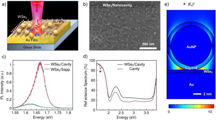
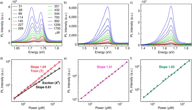
Exciton is a bosonic quasiparticle consisting of a pair of electron and hole, with promising potentials for optoelectronic device applications, such as exciton transistors, photodetectors and light emitting devices. However, the charge-neutral nature of excitons renders them challenging to manipulate using electronics. Here we present the generation of trions, a form of charged excitons, together with enhanced exciton resonance in monolayer WSe2. The excitation of the trion quasiparticles is achieved by the hot carrier transport from the integrated gold plasmonic nanocavity, formed by embedding monolayer WSe2 between gold nanoparticles and a gold film. The nanocavity-induced negatively charged trions provide a promising route for the manipulation of excitons, essential for the construction of all-exciton information processing circuits.


Conflict of interest statement

The authors declare no competing interests.

Figures

Figure 1
Figure 1
Monolayer WSe2 embedded in a plasmonic nanocavity and characterizations. (a) Schematic of monolayer WSe2 embedded in a plasmonic nanocavity comprising gold nanoparticles (AuNPs) and gold-film substrate, with enhanced PL emission being observed. (b) Representative scanning electron microscope (SEM) image of monolayer WSe2 embedded in nanocavity (WSe2/Nanocavity). (c) PL spectra of monolayer WSe2 in nanocavity and monolayer WSe2 on sapphire with an emission peak at 1.67 eV and 1.62 eV, respectively. (d) Reflectance spectra of nanocavity with and without monolayer WSe2. The red dot at 1.68 eV denotes the energy of localized plasmon resonance. (e) Finite-difference time-domain (FDTD) simulation of the enhanced electric displacement intensity, |Ez|2, inside the monolayer WSe2 due to the localized vertical gap plasmons.
Figure 2
Figure 2
PL emission from monolayer WSe2 embedded in different configurations at a temperature of 77 K. The CW pump laser has energy of 2.33 eV (a) and 1.96 eV (b). The configurations consist of plasmonic nanocavity (WSe2/Nanocavity), monolayer WSe2 on gold-film substrate (WSe2/Au Film), monolayer WSe2 on sapphire (WSe2/Sapphire) and pure plasmonic nanocavity (Pure Nanocavity). The PL measurements were conducted with a laser power of 20 μW.
Figure 3
Figure 3
Investigations of the power-dependent PL spectra in different configurations. (a) Power-dependent PL spectra of WSe2/Nanocavity. (b) WSe2/Au Film. (c) WSe2/Sapphire. The excitation laser has energy of 1.96 eV. (df) Integrated PL intensity of WSe2/Nanocavity with left peak from 1.65 to 1.73 eV and right peak integrated from 1.73 to 1.76 eV (d), WSe2/Au Film with peak integrated from 1.55 to 1.77 eV (e), and WSe2/Sapphire with peak integrated from 1.46 to 1.76 eV (f), as a function of laser power.
Figure 4
Figure 4
Temperature-dependent PL characteristics. (a) Temperature-dependent PL emission from exciton (X0) and trion (T) of WSe2/Nanocavity. (b) PL peak position as a function of temperature. Black dots denote the trion peak and red dots denote the exciton peak, which are fitted by dashed lines. The PL was excited by using laser with energy of 1.96 eV and power of 20 μW. (c) Integrated PL intensity of WSe2/Nanocavity with peak integrated from 1.62 to 1.78 eV, as a function of temperature. The decreasing and increasing regimes are denoted in blue and orange, respectively. The intensity evolution revealed a combined effect of phonon scattering and plasmon enhancement.

References

    1. Manzeli S, Ovchinnikov D, Pasquier D, Yazyev OV, Kis A. 2D transition metal dichalcogenides. Nat. Rev. Mater. 2017;2:17033. doi: 10.1038/natrevmats.2017.33. - DOI
    1. Wang Z, et al. Giant photoluminescence enhancement in tungsten-diselenide-gold plasmonic hybrid structures. Nat. Commun. 2016;7:11283. doi: 10.1038/ncomms11283. - DOI - PMC - PubMed
    1. Hu Z, et al. Two-dimensional transition metal dichalcogenides: interface and defect engineering. Chem. Soc. Rev. 2018;47:3100–3128. doi: 10.1039/C8CS00024G. - DOI - PubMed
    1. Lv R, et al. Two-dimensional transition metal dichalcogenides: Clusters, ribbons, sheets and more. Nano Today. 2015;10:559–592. doi: 10.1016/j.nantod.2015.07.004. - DOI
    1. Huang J, Hoang TB, Mikkelsen MH. Probing the origin of excitonic states in monolayer WSe2. Sci. Rep. 2016;6:22414. doi: 10.1038/srep22414. - DOI - PMC - PubMed