. 2022 May 9;30(10):16873-16882.
doi: 10.1364/OE.446507.

Engineering the gain and bandwidth in avalanche photodetectors

Engineering the gain and bandwidth in avalanche photodetectors

Cesar Bartolo-Perez et al. Opt Express. .

Abstract

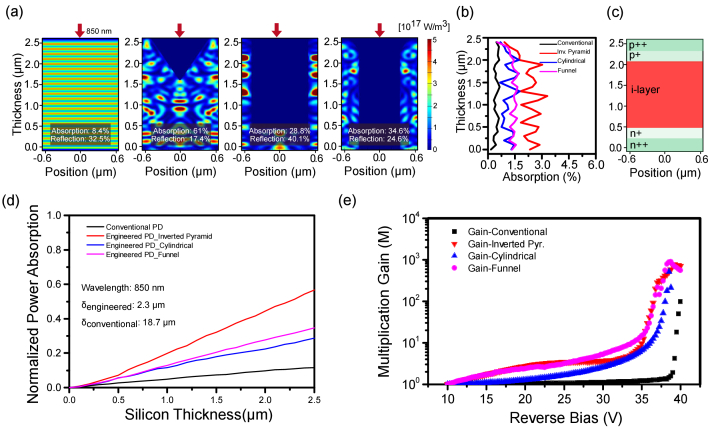
Avalanche and Single-Photon Avalanche photodetectors (APDs and SPADs) rely on the probability of photogenerated carriers to trigger a multiplication process. Photon penetration depth plays a vital role in this process. In silicon APDs, a significant fraction of the short visible wavelengths is absorbed close to the device surface that is typically highly doped to serve as a contact. Most of the photogenerated carriers in this region can be lost by recombination, get slowly transported by diffusion, or multiplied with high excess noise. On the other hand, the extended penetration depth of near-infrared wavelengths requires thick semiconductors for efficient absorption. This diminishes the speed of the devices due to the long transit time in the thick absorption layer that is required for detecting most of these photons. Here, we demonstrate that it is possible to drive photons to a critical depth in a semiconductor film to maximize their gain-bandwidth performance and increase the absorption efficiency. This approach to engineering the penetration depth for different wavelengths in silicon is enabled by integrating photon-trapping nanoholes on the device surface. The penetration depth of short wavelengths such as 450 nm is increased from 0.25 µm to more than 0.62 µm. On the other hand, for a long-wavelength like 850 nm, the penetration depth is reduced from 18.3 µm to only 2.3 µm, decreasing the device transit time considerably. Such capabilities allow increasing the gain in APDs by almost 400× at 450 nm and by almost 9× at 850 nm. This engineering of the penetration depth in APDs would enable device designs requiring higher gain-bandwidth in emerging technologies such as Fluorescence Lifetime Microscopy (FLIM), Time-of-Flight Positron Emission Tomography (TOF-PET), quantum communications systems, and 3D imaging systems.


Conflict of interest statement

The authors declare no conflicts of interest

Figures

Fig. 1.
Fig. 1.
(a) Conventional penetration depth of short and long wavelengths in an avalanche PD structure with separate absorption and multiplication layers. Short wavelengths (such as blue light from 380 nm to 485 nm) are mostly absorbed close to the surface due to their high absorption coefficient. Longer wavelengths (such as red and near-infrared light from 625 nm to 1100 nm) travel deeper into the device. (b) A potential engineered PD with integrated photon trapping nanoholes can modify the penetration depth of the incident light. Shorter wavelengths travel deeper while longer wavelengths can be absorbed at a shorter distance. (c) Generated carrier concentration comparison between w/o holes and w/ holes PD structures both for 450 nm and 850 nm wavelengths.
Fig. 2.
Fig. 2.
(a) Schematic of engineered PD with photon trapping nanoholes with a PIN structure for proof of concept. (b) SEM of fabricated PD. (c) Different photon trapping nanohole profiles to study the penetration depth and gain.
Fig. 3.
Fig. 3.
(a) Power absorption of light at 850 nm wavelength in the conventional and engineered PDs with diverse nanohole profiles, simulated by FDTD. (b) Percentage of absorbed light with respect to. the depth. (c) Schematic of the doping profile of the fabricated PD. (d) Comparison of the penetration depth between conventional (δconventional) and engineered (δengineered) APDs for 850 nm wavelength. δ is reduced from 18.7 µm to 2.3 µm. (e) Experimental multiplication gain measurements: comparison between conventional PD and engineered PDs with different nanohole profiles.
Fig. 4.
Fig. 4.
(a) Power absorption of light at 450 nm wavelengths in the conventional and engineered PDs with different nanohole profiles, simulated by FDTD. (b) Percentage of absorbed light with respect to the depth. (c) Comparison of penetration depth between conventional conventional) and engineered engineered) APD. δ increased from 0.25 µm to 0.75 µm. (d) Experimental multiplication gain measurements comparing conventional PD and engineered PDs. The gain increases by nearly a factor of four hundred, from 11.9 to more than 4000. (e-f) Current-Voltage under dark conditions and illumination for a conventional PD (e), and Engineered PD-Cylindrical with an input light wavelength of 450 nm (f), and 850 nm (g).
Fig. 5.
Fig. 5.
(a) Penetration depth of 450 nm wavelength light in varying photon-trapping nanohole depths. The penetration depth increases with the depth of the hole from 250 nm to 620 nm. (b) Absorption and penetration depth for different hole depths at 450 nm wavelength. A maximum of 84% of absorption can be obtained at 800 nm nanohole depth. (c) Optical absorption profile obtained by FDTD for an incident light of 450 nm.
Fig. 6.
Fig. 6.
(a) Penetration depth engineered on silicon for incident light wavelengths between 300 nm to 700 nm. (b) Comparison of penetration depth between conventional and engineered PDs. At wavelengths below 450 nm, the penetration depth is dramatically increased, reducing the loss of carriers by recombination, slow diffusion transport, and high excess noise multiplication. Above 500 nm wavelength, the penetration depth is reduced by more than 50%. At 850 nm the penetration depth is reduced from 18.3 µm to only 2.3 µm, an 87% reduction in the depth. (c) The power distribution of incident light at different wavelengths on conventional and photon-trapping photodiodes for nanoholes depth of 400 nm, a diameter of 480 nm, and a period of 500 nm.

References

    1. Zhou X., Bec J., Yankelevich D., Marcu L., “Multispectral fluorescence lifetime imaging device with a silicon avalanche photodetector,” Opt. Express 29(13), 20105–20120 (2021).10.1364/OE.425632 - DOI - PMC - PubMed
    1. Bec J., Phipps J. E., Gorpas D., Ma D., Fatakdawala H., Margulies K. B., Southard J. A., Marcu L., “In vivo label-free structural and biochemical imaging of coronary arteries using an integrated ultrasound and multispectral fluorescence lifetime catheter system,” Sci. Rep. 7(1), 8960 (2017).10.1038/s41598-017-08056-0 - DOI - PMC - PubMed
    1. Bruschini C., Homulle H., Antolovic I. M., Burri S., Charbon E., “Single-photon avalanche diode imagers in biophotonics: review and outlook,” Light: Sci. Appl. 8(1), 87 (2019).10.1038/s41377-019-0191-5 - DOI - PMC - PubMed
    1. Bartolo-Perez C., Ghandiparsi S., Mayet A., Cansizoglu H., Gao Y., Qarony W., Ahamed A., Wang S.-Y., Cherry S., Islam M. S., Ariño-Estrada G., “Avalanche Photodetectors with Photon Trapping Structures for Biomedical Imaging Applications,” in 2021), - PMC - PubMed
    1. Huang S., Safari M., “Hybrid SPAD/PD Receiver for Reliable Free-Space Optical Communication,” IEEE Open J. Commun. Soc. 1, 1364–1373 (2020).10.1109/OJCOMS.2020.3023009 - DOI

LinkOut - more resources