. 2022 Oct 26;14(42):48240-48249.
doi: 10.1021/acsami.2c13148. Epub 2022 Oct 14.

Charge Transport Across Au-P3HT-Graphene van der Waals Vertical Heterostructures

Affiliations

Charge Transport Across Au-P3HT-Graphene van der Waals Vertical Heterostructures

Jacopo Oswald et al. ACS Appl Mater Interfaces. .

Abstract

Hybrid van der Waals heterostructures based on 2D materials and/or organic thin films are being evaluated as potential functional devices for a variety of applications. In this context, the graphene/organic semiconductor (Gr/OSC) heterostructure could represent the core element to build future vertical organic transistors based on two back-to-back Gr/OSC diodes sharing a common graphene sheet, which functions as the base electrode. However, the assessment of the Gr/OSC potential still requires a deeper understanding of the charge carrier transport across the interface as well as the development of wafer-scale fabrication methods. This work investigates the charge injection and transport across Au/OSC/Gr vertical heterostructures, focusing on poly(3-hexylthiophen-2,5-diyl) as the OSC, where the PMMA-free graphene layer functions as the top electrode. The structures are fabricated using a combination of processes widely exploited in semiconductor manufacturing and therefore are suited for industrial upscaling. Temperature-dependent current-voltage measurements and impedance spectroscopy show that the charge transport across both device interfaces is injection-limited by thermionic emission at high bias, while it is space charge limited at low bias, and that the P3HT can be assumed fully depleted in the high bias regime. From the space charge limited model, the out-of-plane charge carrier mobility in P3HT is found to be equal to μ ≈ 2.8 × 10⁻⁴ cm2 V-1 s-1, similar to the in-plane mobility reported in previous works, while the charge carrier density is N0 ≈ 1.16 × 1015 cm-3, also in agreement with previously reported values. From the thermionic emission model, the energy barriers at the Gr/P3HT and Au/P3HT interfaces result in 0.30 eV and 0.25 eV, respectively. Based on the measured barriers heights, the energy band diagram of the vertical heterostructure is proposed under the hypothesis that P3HT is fully depleted.

Keywords: graphene; interface; organic; semiconductor; transport; van der Waals; vertical.


Conflict of interest statement

The authors declare no competing financial interest.

Figures
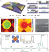
Figure 1
Figure 1
(a) 3D schematic of a representative Au/P3HT/Gr heterostructure (not to scale). (b) Schematic of the fabrication process. AFM (c) height and (d) phase images of a representative 20 μm device. (e) SEM of a FIB cut cross-section of a representative Au/P3HT/Gr heterostructure in the center of the device. (f) Raman spectra of P3HT powder (blue line) and of a representative Au/P3HT/Gr device (dashed green line). The optical image shows the acquisition position of the spectra (the red scale bar is 10 μm). The inset shows the Raman spectra of a device graphene against the Raman spectrum of a representative CVD graphene on SiO2.
Figure 2
Figure 2
(a) Device schematics and electrical schemes of the Au/P3HT/Gr stack and of the graphene bridge devices. Rs is the graphene series resistance, R is the out-of-plane resistance, and C is the geometrical capacitance of the device. (b) Distribution of Rs in vacuum and in vacuum after annealing (17 samples). The inset shows two representative IV traces of side-contacted graphene. The resistance is calculated from the linear fit (dashed lines). (c) Current density of representative devices with diameter 5, 10, 15, 20, 25, 30, and 50 μm. The inset shows the same traces on log scale. (d) Temperature-dependent JV characteristic of a 5 μm device from 200 to 300 K in steps of 5 K. The inset shows the Richardson plot for 5 V and −5 V.
Figure 3
Figure 3
Impedance analysis. (a) Modulus and (b) phase of a representative 20 μm device: data (circles), R||C model fit (dashed lines) (c) Resistance R and capacitance C extracted from the R||C model fit at different biases. R and C are not calculated in the SCL region and for V < −7.5 V, where the cutoff frequency fc is outside the measurement range. (d) Extracted R and C values for the devices with diameter: 5, 10, 15, 20, 25, 30, and 50 μm. The green dashed line is the linear fit of the capacitance vs area. (e) ϵr vs device diameter (error bars calculated as described in the Supporting Information).
Figure 4
Figure 4
(a) Current density across a 20 μm device. Raw data are represented by gray circles. Processed data (orange and blue circles) takes into account for the graphene series resistance. The graph shows the fitting results of the SCL current (green dashed lines) and TE (red dashed lines). The inset shows the ±1 V region where the space-charge effect is limiting the current across the heterostructure. (b) Current density shown in logarithmic scale. The current density for positive and negative biases is represented by orange and blue circles, respectively. (c) Band diagram of the Au/P3HT/Gr heterojunction illustrating the charge transport regimes and equivalent circuit. The shaded Schottky diodes are forward biased.

References

    1. Gobbi M.; Orgiu E.; Samorì P. When 2D Materials Meet Molecules: Opportunities and Challenges of Hybrid Organic/Inorganic van Der Waals Heterostructures. Adv. Mater. 2018, 30 (18), 1706103.10.1002/adma.201706103. - DOI - PubMed
    1. Jariwala D.; Marks T. J.; Hersam M. C. Mixed-Dimensional van Der Waals Heterostructures. Nat. Mater. 2017, 16 (2), 170–181. 10.1038/nmat4703. - DOI - PubMed
    1. Lee G.-H.; Lee C.-H.; van der Zande A. M.; Han M.; Cui X.; Arefe G.; Nuckolls C.; Heinz T. F.; Hone J.; Kim P. Heterostructures Based on Inorganic and Organic van Der Waals Systems. APL Mater. 2014, 2 (9), 092511.10.1063/1.4894435. - DOI - PubMed
    1. Wang Y.; Tong S. W.; Xu X. F.; Özyilmaz B.; Loh K. P. Interface Engineering of Layer-by-Layer Stacked Graphene Anodes for High-Performance Organic Solar Cells. Adv. Mater. 2011, 23 (13), 1514–1518. 10.1002/adma.201003673. - DOI - PubMed
    1. Park H.; Rowehl J. A.; Kim K. K.; Bulovic V.; Kong J. Doped Graphene Electrodes for Organic Solar Cells. Nanotechnology 2010, 21 (50), 505204.10.1088/0957-4484/21/50/505204. - DOI - PubMed