

Thermo-optic tuning of silicon nitride microring resonators with low loss non-volatile [Formula: see text] phase change material
- PMID: 36280699
- PMCID: PMC9592623
- DOI: 10.1038/s41598-022-21590-w
Thermo-optic tuning of silicon nitride microring resonators with low loss non-volatile [Formula: see text] phase change material
Abstract
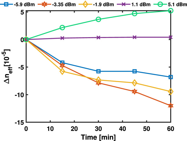
A new family of phase change material based on antimony has recently been explored for applications in near-IR tunable photonics due to its wide bandgap, manifested as broadband transparency from visible to NIR wavelengths. Here, we characterize [Formula: see text] optically and demonstrate the integration of this phase change material in a silicon nitride platform using a microring resonator that can be thermally tuned using the amorphous and crystalline states of the phase change material, achieving extinction ratios of up to 18 dB in the C-band. We extract the thermo-optic coefficient of the amorphous and crystalline states of the [Formula: see text] to be 3.4 x [Formula: see text] and 0.1 x 10[Formula: see text], respectively. Additionally, we detail the first observation of bi-directional shifting for permanent trimming of a non-volatile switch using continuous wave (CW) laser exposure ([Formula: see text] to 5.1 dBm) with a modulation in effective refractive index ranging from +5.23 x [Formula: see text] to [Formula: see text] x 10[Formula: see text]. This work experimentally verifies optical phase modifications and permanent trimming of [Formula: see text], enabling potential applications such as optically controlled memories and weights for neuromorphic architecture and high density switch matrix using a multi-layer PECVD based photonic integrated circuit.
© 2022. The Author(s).
Conflict of interest statement
The authors declare no competing interests.
Figures


References
-
- Lim AE-J, et al. Review of silicon photonics foundry efforts. IEEE J. Sel. Top. Quant. Electron. 2013;20:405–416.
-
- Soref R. Mid-infrared photonics in silicon and germanium. Nat. Photonics. 2010;4:495–497.
-
- Tait AN, et al. Silicon photonic modulator neuron. Phys. Rev. Appl. 2019;11:064043. doi: 10.1103/PhysRevApplied.11.064043. - DOI
-
- Willner AE, et al. Optics and photonics: Key enabling technologies. Proc. IEEE. 2012;100:1604–1643.
-
- Qiang X, et al. Large-scale silicon quantum photonics implementing arbitrary two-qubit processing. Nat. Photonics. 2018;12:534–539.
Grants and funding
- EP/R003076/1/Engineering and Physical Sciences Research Council
- EP/M015130/1/Engineering and Physical Sciences Research Council
- EP/R003076/1/Engineering and Physical Sciences Research Council
- EP/R003076/1/Engineering and Physical Sciences Research Council
- EP/M015130/1/Engineering and Physical Sciences Research Council
LinkOut - more resources
Full Text Sources
Miscellaneous
