

An Ultra-Compact MEMS Pirani Sensor for In-Situ Pressure Distribution Monitoring
- PMID: 36296039
- PMCID: PMC9611872
- DOI: 10.3390/mi13101686
An Ultra-Compact MEMS Pirani Sensor for In-Situ Pressure Distribution Monitoring
Abstract
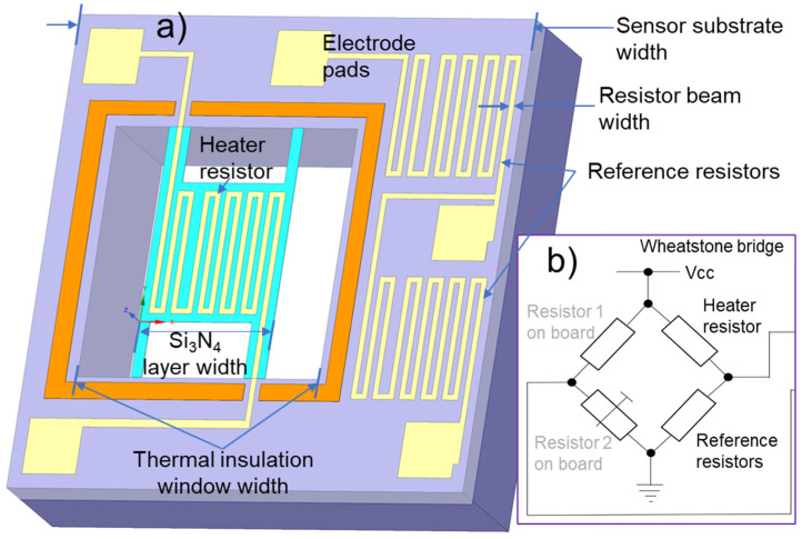
In this study, we designed a microelectromechanical system (MEMS) Pirani vacuum sensor with a compact size. Specifically, the sensor was successfully fabricated based on the Pirani principle and using a commercial eight-inch MEMS foundry process. The sensor fabrication process was carried out using only four photomasks and the proposed sensor had an ultra-compact fabricated size (<2.2 × 2.2 mm2). A vacuum measurement system was set up to comprehensively evaluate the fabricated sensors. The results demonstrated that the MEMS Pirani vacuum sensor has a high responsivity in the low-pressure domain from 100 Pa. The proposed sensor with a 953.0-Ω heater exhibited an average responsivity of 11.9 mV/Pa in the preferred range of 100 to 7 Pa and 96.0 mV/Pa in the range of 7 to 1 Pa. The sensor may be potentially suitable in many applications, such as vacuum indicators for processing equipment, health monitoring systems for social infrastructure, and medical and health applications.
Keywords: MEMS; Pirani sensor; lift-off; simple process; vacuum test.
Conflict of interest statement
The authors declare no conflict of interest.
Figures


Similar articles
-
A Composite-Type MEMS Pirani Gauge for Wide Range and High Accuracy.Sensors (Basel). 2023 Jan 22;23(3):1276. doi: 10.3390/s23031276. Sensors (Basel). 2023. PMID: 36772316 Free PMC article.
-
Overview of the MEMS Pirani Sensors.Micromachines (Basel). 2022 Jun 14;13(6):945. doi: 10.3390/mi13060945. Micromachines (Basel). 2022. PMID: 35744559 Free PMC article. Review.
-
Highly Sensitive Diode-Based Micro-Pirani Vacuum Sensor with Low Power Consumption.Sensors (Basel). 2019 Jan 7;19(1):188. doi: 10.3390/s19010188. Sensors (Basel). 2019. PMID: 30621043 Free PMC article.
-
A MEMS Pirani Vacuum Gauge Based on Porous Silicon.Micromachines (Basel). 2025 Feb 28;16(3):296. doi: 10.3390/mi16030296. Micromachines (Basel). 2025. PMID: 40141908 Free PMC article.
-
Recent Advances of MEMS Resonators for Lorentz Force Based Magnetic Field Sensors: Design, Applications and Challenges.Sensors (Basel). 2016 Aug 24;16(9):1359. doi: 10.3390/s16091359. Sensors (Basel). 2016. PMID: 27563912 Free PMC article. Review.
References
-
- O’Hanlon J.F., Parks H.G. Impact of vacuum equipment contamination on semiconductor yield. J. Vac. Sci. Technol. A. 1992;10:1863–1868. doi: 10.1116/1.577760. - DOI
-
- Hasegawa H., Ohno H. Unified disorder induced gap state model for insulator–semiconductor and metal–semiconductor interfaces. J. Vac. Sci. Technol. B. 1998;4:1130–1138. doi: 10.1116/1.583556. - DOI
-
- Lessard P.A. Dry vacuum pumps for semiconductor processes: Guidelines for primary pump selection. J. Vac. Sci. Technol. A. 2000;18:1777–1781. doi: 10.1116/1.582423. - DOI
-
- Pirani M.S. Selbstzeigendes vakuum-messinstrument. Dtsch. Phys. Ges. Verh. 1906;8:686–694.
-
- Shie J.S., Chou B.C.S., Chen Y.M. High performance Pirani vacuum gauge. J. Vac. Sci. Technol. A. 1995;13:2972–2979. doi: 10.1116/1.579623. - DOI
LinkOut - more resources
Full Text Sources
