. 2022 Oct 13;12(20):3585.
doi: 10.3390/nano12203585.

Nanostructured MoS2 and WS2 Photoresponses under Gas Stimuli

Affiliations

Nanostructured MoS2 and WS2 Photoresponses under Gas Stimuli

Mohamed A Basyooni et al. Nanomaterials (Basel). .

Abstract

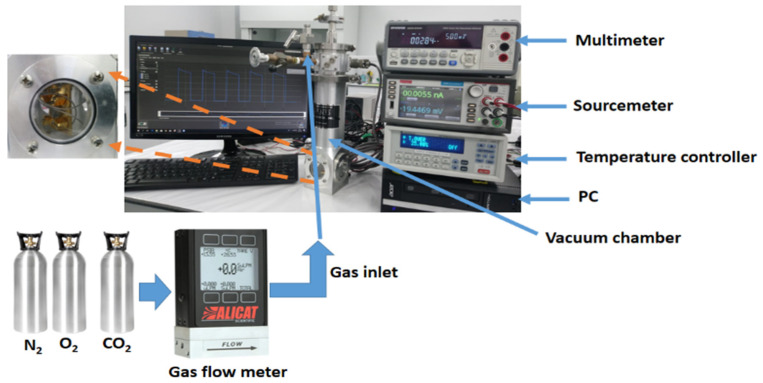
This study was on the optoelectronic properties of multilayered two-dimensional MoS2 and WS2 materials on a silicon substrate using sputtering physical vapor deposition (PVD) and chemical vapor deposition (CVD) techniques. For the first time, we report ultraviolet (UV) photoresponses under air, CO2, and O2 environments at different flow rates. The electrical Hall effect measurement showed the existence of MoS2 (n-type)/Si (p-type) and WS2 (P-type)/Si (p-type) heterojunctions with a higher sheet carrier concentration of 5.50 × 105 cm-2 for WS2 thin film. The IV electrical results revealed that WS2 is more reactive than MoS2 film under different gas stimuli. WS2 film showed high stability under different bias voltages, even at zero bias voltage, due to the noticeably good carrier mobility of 29.8 × 102 cm2/V. WS2 film indicated a fast rise/decay time of 0.23/0.21 s under air while a faster response of 0.190/0.10 s under a CO2 environment was observed. Additionally, the external quantum efficiency of WS2 revealed a remarkable enhancement in the CO2 environment of 1.62 × 10⁸ compared to MoS2 film with 6.74 × 10⁶. According to our findings, the presence of CO2 on the surface of WS2 improves such optoelectronic properties as photocurrent gain, photoresponsivity, external quantum efficiency, and detectivity. These results indicate potential applications of WS2 as a photodetector under gas stimuli for future optoelectronic applications.

Keywords: MoS2; WS2; optoelectronics; thin film; two-dimensional material.


Conflict of interest statement

The authors declare no conflict of interest.

Figures

Scheme 1
Scheme 1
Electrical and optoelectrical systems under different gas environments and different temperature conditions.
Figure 1
Figure 1
(a,b) Raman spectra of MoS2 and WS2 on Si substrates, respectively.
Figure 2
Figure 2
(a,b) PL spectra of MoS2 and WS2 on Si substrates, respectively.
Figure 3
Figure 3
(a) MoS2 and (b) WS2 thin-film optical microscopy images.
Figure 4
Figure 4
(a,b) FE-SEM morphology of MoS2 and WS2 thin films.
Figure 5
Figure 5
AFM topography and the horizontal line profile: (a,b) 3D topography images and corresponding line profile of MoS2 and WS2 samples, respectively.
Figure 6
Figure 6
(a,b) General XPS survey spectrum distributions of both MoS2 and WS2 thin films.
Figure 7
Figure 7
The MoS2 and WS2 photodetector under the illumination of UV light and the device’s actual image as seen through the probe station. The measurements were carried out in the air, O2, and CO2 environments.
Figure 8
Figure 8
I-V characteristic of MoS2 in the absence of light and UV illumination conditions under air and CO2.
Figure 9
Figure 9
(a) Photocurrent behavior with time of MoS2 under dark and UV illumination conditions in air, and (b) the on–off time-resolved photoresponse of MoS2 thin film under bias voltages of 0–5 V.
Figure 10
Figure 10
(a,b) Photocurrent behavior with time and on–off time-resolved photoresponse of MoS2 thin film under dark and UV illumination conditions in both air and 50 sccm CO2 environments at a bias voltage of 5 V.
Figure 11
Figure 11
Characteristic I-V curve of WS2 under dark and UV illumination conditions under (a) air environment, (b) O2 environment and (c) CO2 environment.
Figure 11
Figure 11
Characteristic I-V curve of WS2 under dark and UV illumination conditions under (a) air environment, (b) O2 environment and (c) CO2 environment.
Figure 12
Figure 12
(a) Photocurrent behavior with the time of WS2 thin film under a dark condition in the air at a different bias voltage of 0, 0.5, 1, and 2 V. (b) The on–off dynamics of the current with a time of WS2 thin film in air and 50 sccm O2 environments under a different bias voltage of 0–2 V.
Figure 13
Figure 13
(a) Photocurrent behavior with time of WS2 thin film under dark and UV conditions in CO2 at a bias voltage of 2 V. (b) The on–off dynamics of the photoresponse with a time of WS2 thin film in air, 50 sccm O2, and 50 sccm CO2 environments under a bias voltage of 2 V.
Figure 14
Figure 14
Shows the response and therecovery times for (a) MoS2 and (b) WS2 thin films under gas stimuli.
Figure 15
Figure 15
(a,b) Photocurrent and photocurrent gain of MoS2 and WS2 thin film under gas stimuli.

References

    1. Gonzaalez-Cuevas J.A., Refaat T.F., Abedin M.N., Elsayed-Ali H.E. Modeling of the Temperature-Dependent Spectral Response of In_{1−x}Ga_{x}Sb Infrared Photodetectors. Opt. Eng. 2006;45:44001.
    1. Basyooni M.A., Shaban M., El Sayed A.M. Enhanced Gas Sensing Properties of Spin-coated Na-doped ZnO Nanostructured Films. Sci. Rep. 2017;7:41716. doi: 10.1038/srep41716. - DOI - PMC - PubMed
    1. Zaki S.E., Basyooni M.A. Ultra-sensitive gas sensor based fano resonance modes in periodic and fibonacci quasi-periodic Pt/PtS2 structures. Sci. Rep. 2022;12:9759. doi: 10.1038/s41598-022-13898-4. - DOI - PMC - PubMed
    1. Zaki S.E., Basyooni M.A., Shaban M., Rabia M., Eker Y.R., Attia G.F., Yilmaz M., Ahmed A.M. Role of oxygen vacancies in vanadium oxide and oxygen functional groups in graphene oxide for room temperature CO2 gas sensors. Sens. Actuators A Phys. 2019;294:17–24. doi: 10.1016/j.sna.2019.04.037. - DOI
    1. Owen T. The Composition and Early History of the Atmosphere of Mars. Mars Publication; Hong Kong, China: 2018. pp. 818–834.

LinkOut - more resources