. 2022 Oct 27;13(1):6404.
doi: 10.1038/s41467-022-34170-3.

Strongly enhanced THz generation enabled by a graphene hot-carrier fast lane

Affiliations

Strongly enhanced THz generation enabled by a graphene hot-carrier fast lane

Dehui Zhang et al. Nat Commun. .

Abstract

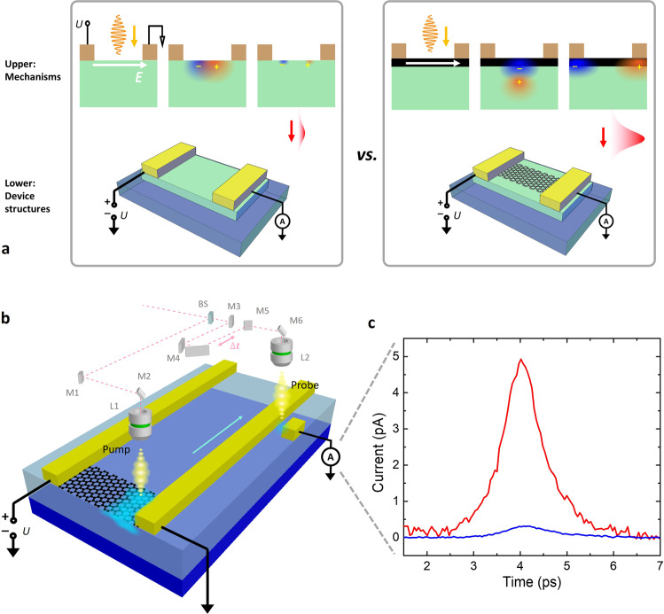
Semiconductor photoconductive switches are useful and versatile emitters of terahertz (THz) radiation with a broad range of applications in THz imaging and time-domain spectroscopy. One fundamental challenge for achieving efficient ultrafast switching, however, is the relatively long carrier lifetime in most common semiconductors. To obtain picosecond ultrafast pulses, especially when coupled with waveguides/transmission lines, semiconductors are typically engineered with high defect density to reduce the carrier lifetimes, which in turn lowers the overall power output of the photoconductive switches. To overcome this fundamental trade-off, here we present a new hybrid photoconductive switch design by engineering a hot-carrier fast lane using graphene on silicon. While photoexcited carriers are generated in the silicon layer, similar to a conventional switch, the hot carriers are transferred to the graphene layer for efficient collection at the contacts. As a result, the graphene-silicon hybrid photoconductive switch emits THz fields with up to 80 times amplitude enhancement compared to its graphene-free counterpart. These results both further the understanding of ultrafast hot carrier transport in such hybrid systems and lay the groundwork toward intrinsically more powerful THz devices based on 2D-3D hybrid heterostructures.


Conflict of interest statement

The authors declare no competing interests.

Figures

Fig. 1
Fig. 1. Schematic illustration of the THz emitter with graphene as the hot carrier fast lane.
a Structure of the conventional PCS without graphene (left box, lower panel) versus the device with graphene (right box, lower panel). The corresponding THz field generation mechanism is shown in the upper panels. Hot carriers are majorly generated in O + ion-implanted silicon (green). Hot carriers separate more efficiently in the graphene layer (black) than in the silicon layer, hence creating a stronger THz field on the right. b The on-chip pump–probe measurement setup. The beam splitter (BS) separates the input beam into pump and probe beams. A motorized stage controls the time delay (mirror M4) of the two beams, which are focused to hit the sample at the emitter (through L1) and the detector (through L2) respectively. A transmission line is used to couple the field to an Auston switch (detector). c Strongly enhanced THz field observed from our hybrid device (red) over graphene-free device (navy). The channel bias is 6 V, with a pump power of 3 mW and probe power of 10 mW for both emitters.
Fig. 2
Fig. 2. Measured field enhancement and data analysis.
a Time-resolved measurement of received field amplitude under different channel bias, with pump power of 3 mW and probe power of 10 mW. Violet to red (following the gray arrow): channel bias = 1 to 9 V with a 1 V stepped increase. Pink: graphene-free device at 9 V. b Gain of generation (measured in power) compared to graphene-free device at identical test conditions. The power gain varies from 19 to 38 dB at different channel bias and pump power (pump powers marked in the graph, unit: mW). c Extracted rise and fall times of the pulses with τ value from least-square-regression Gaussian fitting. Red: rise time, graphene on silicon device; orange: fall time, graphene on silicon device; navy: rise time, silicon device; blue: fall time, silicon device. d Fourier-transformed THz spectrum of graphene device (red dot) and graphene-free device (blue circle). The data in c and d are extracted from a, which shows no decrease in bandwidth or SNR.
Fig. 3
Fig. 3. Experimental data for field generation mechanism analysis.
a THz field from a pure graphene device under different channel bias (brown: 0 V; red: 4 V; orange: 8 V), with pump power = 5 mW and probe power = 30 mW. b THz field from the same 2D–3D heterostructure with a lightly implanted silicon substrate. Black to yellow: channel bias from 3 V to 9 V with 1 V step increase (gray arrow). c Extracted rise (navy) and fall (red) time through Gaussian fit. A comparison is made with the heavily implanted ones (green banner).
Fig. 4
Fig. 4. Gate dependence of device performance.
a Current across the device under 1 V channel bias (U) and sweeping gate bias (Vg). Inset: electrical operation for dark current in a and scanning beam measurements in b. b Spatial scanned pump beam is used to probe the photocurrent at U = 0 V. The amplitude (upper) and phase (lower) are plotted with respect to both position and gate bias. c The proposed band alignment of the device, with silicon surface depleted at negative gate bias and accumulation at positive gate bias. At large positive Vg, the band distortion to silicon electron accumulation counter-dopes the graphene layer. d Gate dependence of the peak THz pulse amplitude from the device, with error bars (determined by the standard deviations) and signals from the lock-in amplifier’s X (red) and Y (blue) channels, indicating a stable phase of the THz field.

Similar articles

Cited by

  • A hot-emitter transistor based on stimulated emission of heated carriers.
    Liu C, Wang XZ, Shen C, Ma LP, Yang XQ, Kong Y, Ma W, Liang Y, Feng S, Wang XY, Wei YN, Zhu X, Li B, Li CZ, Dong SC, Zhang LN, Ren WC, Sun DM, Cheng HM. Liu C, et al. Nature. 2024 Aug;632(8026):782-787. doi: 10.1038/s41586-024-07785-3. Epub 2024 Aug 14. Nature. 2024. PMID: 39143208 Free PMC article.

References

    1. Malhotra I, Jha KR, Singh G. Terahertz antenna technology for imaging applications: a technical review. Int. J. Microw. Wirel. Technol. 2018;10:271–290.
    1. Kemp MC, et al. Security applications of terahertz technology. Int. Soc. Opt. Photonics. 2003;5070:44–52.
    1. Federici JF, et al. THz imaging and sensing for security applications—explosives, weapons and drugs. Semicond. Sci. Technol. 2005;20:S266.
    1. Liu HB, et al. Terahertz spectroscopy and imaging for defense and security applications. Proc. IEEE. 2007;95:1514–1527.
    1. Ho L, Pepper M, Taday P. Terahertz spectroscopy: signatures and fingerprints. Nat. Photonics. 2008;2:541.