

Wafer-Scale Room-Temperature Bonding of Smooth Au/Ti-Based Getter Layer for Vacuum Packaging
- PMID: 36365842
- PMCID: PMC9658547
- DOI: 10.3390/s22218144
Wafer-Scale Room-Temperature Bonding of Smooth Au/Ti-Based Getter Layer for Vacuum Packaging
Abstract
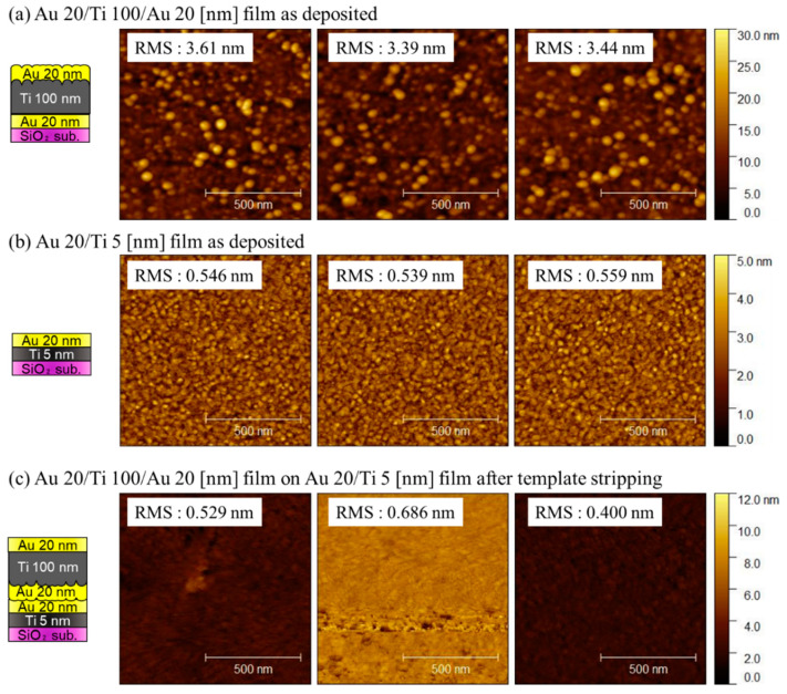
This study demonstrates room-temperature bonding using a getter layer for the vacuum packaging of microsystems. A thick Ti layer covered with an Au layer is utilized as a getter layer because it can absorb gas molecules in the package. Additionally, smooth Au surfaces can form direct bonds for hermetic sealing at room temperature. Direct bonding using a getter layer can simplify the vacuum packaging process; however, typical getter layers are rough in bonding formation. This study demonstrates two fabrication techniques for smooth getter layers. In the first approach, the Au/Ti layer is bonded to an Au layer on a smooth SiO2 template, and the Au/SiO2 interface is mechanically exfoliated. Although the root-mean-square roughness was reduced from 2.00 to 0.98 nm, the surface was still extremely rough for direct bonding. In the second approach, an Au/Ti/Au multilayer on a smooth SiO2 template is bonded with a packaging substrate, and the Au/SiO2 interface is exfoliated. The transferred Au/Ti/Au getter layer has a smooth surface with the root-mean-square roughness of 0.54 nm and could form wafer-scale direct bonding at room temperature. We believe that the second approach would allow a simple packaging process using direct bonding of the getter layer.
Keywords: getter layer; room-temperature bonding; template stripping; wafer-scale packaging.
Conflict of interest statement
The authors declare that they have no competing interests.
Figures


References
-
- Kim J., Jeong B., Chiao M., Lin L. Ultrasonic Bonding for MEMS Sealing and Packaging. IEEE Trans. Adv. Packag. 2009;32:461–467. doi: 10.1109/TADVP.2008.2009927. - DOI
-
- Dhayal M., Jeong H.G., Choi J.S. Use of Plasma Polymerisation Process for Fabrication of Bio-MEMS for Micro-Fluidic Devices. Appl. Surf. Sci. 2005;252:1710–1715. doi: 10.1016/j.apsusc.2005.03.198. - DOI
-
- Knechtel R. Low Temperature Wafer Bonding for MEMS Processes and 3D Integration; Proceedings of the 2012 3rd IEEE International Workshop on Low Temperature Bonding for 3D Integration; Tokyo, Japan. 22–23 May 2012; pp. 258–262. - DOI
-
- Takigawa R., Higurashi E., Suga T., Sawada R. Room-Temperature Bonding of Vertical-Cavity Surface-Emitting Laser Chips on Si Substrates Using Au Microbumps in Ambient Air. Appl. Phys. Express. 2008;1:1122011–1122012. doi: 10.1143/APEX.1.112201. - DOI
-
- Lee C., Yu A., Yan L., Wang H., He J.H., Zhang Q.X., Lau J.H. Characterization of Intermediate In/Ag Layers of Low Temperature Fluxless Solder Based Wafer Bonding for MEMS Packaging. Sensors Actuators A Phys. 2009;154:85–91. doi: 10.1016/j.sna.2008.10.011. - DOI
Grants and funding
LinkOut - more resources
Full Text Sources
