. 2022 Nov 19;20(1):491.
doi: 10.1186/s12951-022-01684-3.

Filtration-processed biomass nanofiber electrodes for flexible bioelectronics

Affiliations

Filtration-processed biomass nanofiber electrodes for flexible bioelectronics

Daiki Ando et al. J Nanobiotechnology. .

Abstract

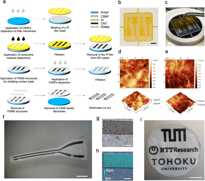
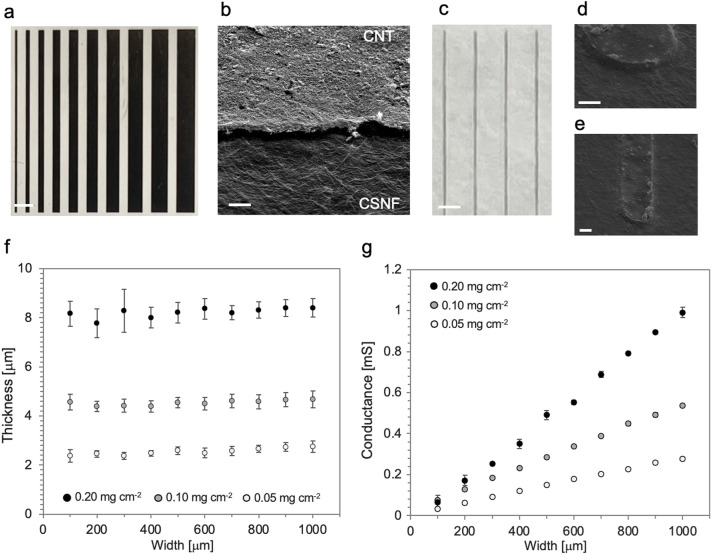
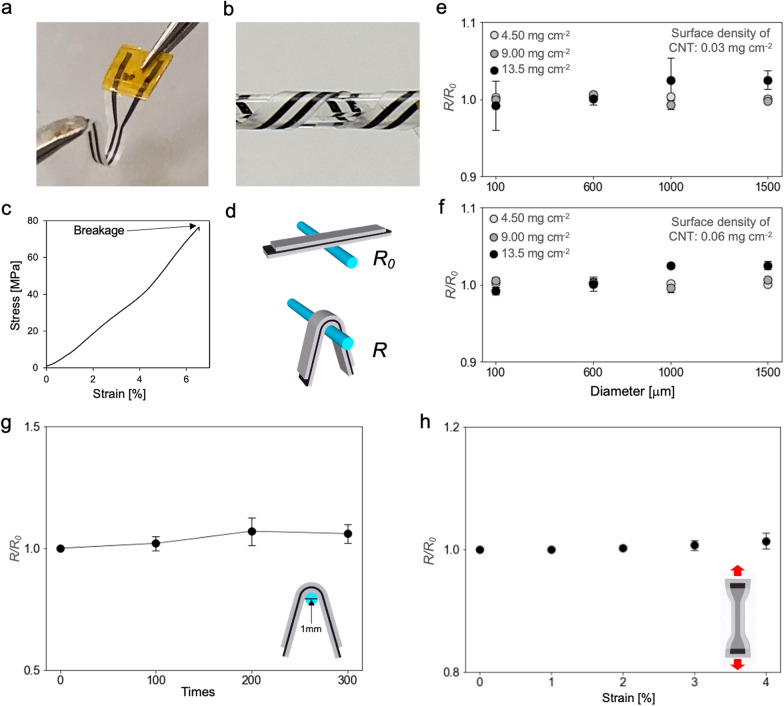
An increasing demand for bioelectronics that interface with living systems has driven the development of materials to resolve mismatches between electronic devices and biological tissues. So far, a variety of different polymers have been used as substrates for bioelectronics. Especially, biopolymers have been investigated as next-generation materials for bioelectronics because they possess interesting characteristics such as high biocompatibility, biodegradability, and sustainability. However, their range of applications has been restricted due to the limited compatibility of classical fabrication methods with such biopolymers. Here, we introduce a fabrication process for thin and large-area films of chitosan nanofibers (CSNFs) integrated with conductive materials. To this end, we pattern carbon nanotubes (CNTs), silver nanowires, and poly (3,4-ethylenedioxythiophene):poly (styrenesulfonate) (PEDOT:PSS) by a facile filtration process that uses polyimide masks fabricated via laser ablation. This method yields feedlines of conductive material on nanofiber paper and demonstrates compatibility with conjugated and high-aspect-ratio materials. Furthermore, we fabricate a CNT neural interface electrode by taking advantage of this fabrication process and demonstrate peripheral nerve stimulation to the rapid extensor nerve of a live locust. The presented method might pave the way for future bioelectronic devices based on biopolymer nanofibers.

Keywords: Bioelectronics; Biopolymers; High-aspect-ratio materials; Implantable Electrodes; Membrane filtration.


Conflict of interest statement

The authors declare no competing interests.

Figures

Fig. 1
Fig. 1
Fabrication process for CSNF-based electrodes for peripheral nerve stimulation. a Schematic of the fabrication process of CSNF paper electrodes. b, c Images of laser-patterned PI masks. PI masks are directly patterned by a laser ablation process (b), and removed gently after filtration to fabricate CNT micropatterns (c). d, e AFM images of the CSNF (d), and CNT network on CSNF (e). f An image of a CSNF paper electrode for in vivo experiments. g, h Laser-scanned 3D images of the surface topology of the electrode that is used for in vivo experiments. i An example of a patterned paper electrode without passivation. Scale bars: (b) 5 mm, (f) 2.5 mm (g, h) 100 µm (i) 1 cm
Fig. 2
Fig. 2
Characteristics of CNT feedlines embedded in CSNF papers. a CNT feedlines with 100-1000 µm in width and 1 cm in length, respectively. b An SEM image of the border between CNT networks and CSNF paper substrates. c CNT feedlines 25 µm in width. d, e SEM images of image (c). f, g The thicknesses and conductance of CNT feedlines dependent on the different surface densities (black dots: 0.2 mg cm−2, gray dots: 0.1 mg cm−2, white dots: 0.05 mg cm−2) and width of feedlines. The average thicknesses (n = 18, mean ± standard deviation) (f) and the conductance of CNT feedlines (n = 3, mean ± standard deviation) (g). Scale bars: a, c 1 mm, b 5 µm, d, e 10 µm
Fig. 3
Fig. 3
Characteristics of various conductive materials embedded in CSNF substrates. a SEM image of the border between AgNW networks and CSNF paper. b carboxymethylcellulose nanofiber aggregations entangled in AgNW networks. c Conductance of AgNW feedlines with different surface densities (black dots: 0.2 mg cm−2, gray dots: 0.1 mg cm−2, white dots: 0.05 mg cm−2, n = 6, mean ± standard deviation). d, e SEM images of a border between PEDOT:PSS and the CSNF substrate d and between CNT/PEDOT:PSS composites and the CSNF substrate. f Conductance of CNT (circle dots), PEDOT:PSS (triangle dots), and CNT/PEDOT:PSS composite feedlines (diamond dots). (n = 5, mean ± standard deviation). Scale bars: a, d, e 5 µm, (b) 2 µm
Fig. 4
Fig. 4
Changes in resistances against mechanical deformation with CNT/CSNF electrodes. a Image of a CNT/CSNF electrode fabricated for in vivo experiments. b The electrode was bent and wrapped around a glass rod (1 mm in diameter). c An exemplary stress–strain curve of a CNT/CSNF electrode. d Schematics of resistance measurements with CNT/CSNF electrodes before and while being wrapped around the glass rods. e, f Relative resistance of CNT/CSNF electrodes with different surface density of CNTs and CSNF wrapped around glass rods (n = 3, mean ± standard deviation). The surface density of CNT are 0.03 mg cm−2 (e) and 0.06 mg cm−2 (f), respectively, and the electrodes have three varieties of CSNF density with 4.5 mg cm−2 (white dots), 9.0 mg cm−2 (gray dots) and 13.5 mg cm.−2 (black dots). g Relative resistance of CNT/CSNF electrodes in dependence on bending cycles (n = 3, mean ± standard deviation). h Relative resistance of CNT/CSNF electrodes during strain applicatioin (n = 4, mean ± standard deviation)
Fig. 5
Fig. 5
Electrochemical characterization of CNT/CSNF electrodes. a Cyclic voltammograms for the CNT/CSNF electrodes sweeping from -2 V to 2 V vs Ag/AgCl to determine the water window. b Impedance spectroscopy for the electrodes (n = 8, mean ± standard deviation)
Fig. 6
Fig. 6
in vivo implantation of the electrodes using locusts. a, b Image of the N5 of the locust. b A CNT/CSNF electrode interfaces with the N5 of the locust. c A schematic drawing of the interface between a CNT/CSNF electrode and an N5 of a locust. d An image showing the locust-tibia extension with the corresponding change in angle. e The trace of the angle measured during application of 220 µA double biphasic pulses every 5 s. f The angle of the locust-tibia extensions caused by stimulations (n = 15, mean ± standard deviation)

References

    1. Nawaz A, Liu Q, Leong WL, Fairfull-Smith KE, Sonar P. Organic electrochemical transistors for in vivo bioelectronics. Adv Mater. 2021;33:2101874. - PubMed
    1. Chadha U, Bhardwaj P, Agarwal R, Rawat P, Agarwal R, Gupta I, Panjwani M, Singh S, Ahuja C, Selvaraj SK, Banavoth M, Sonar P, Badoni B, Chakravorty A. Recent progress and growth in biosensors technology: a critical review. J Indust Engineer Chem. 2022;109:21–51.
    1. Ren Z, Yang J, Qi D, Sonar P, Liu L, Lou Z, Shen G, Wei Z. Flexible sensors based on organic–inorganic hybrid materials. Adv Mater Technol. 2021;6:2000889.
    1. Someya T, Bao Z, Malliaras GG. The rise of plastic bioelectronics. Nature. 2016;540:379–385. - PubMed
    1. Irimia-Vladu M. “Green” electronics: biodegradable and biocompatible materials and devices for sustainable future. Chem Soc Rev. 2014;43:588–610. - PubMed

LinkOut - more resources