Fabrication methods for high reflectance dielectric-metal point contact rear mirror for optoelectronic devices
- PMID: 36411803
- PMCID: PMC9674894
- DOI: 10.1016/j.mex.2022.101898
Fabrication methods for high reflectance dielectric-metal point contact rear mirror for optoelectronic devices
Abstract
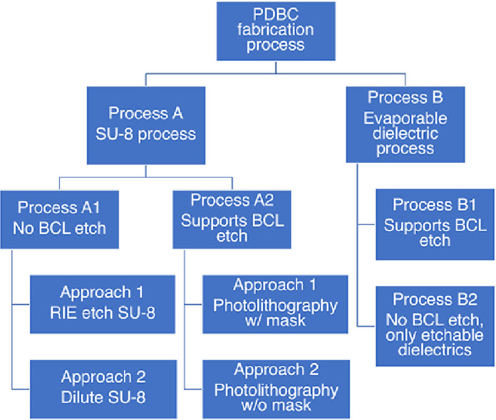
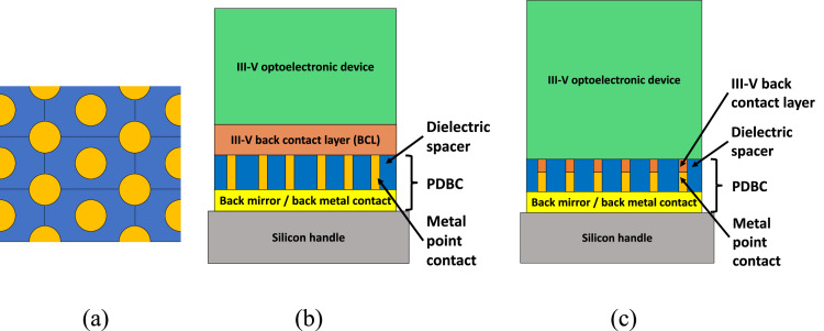
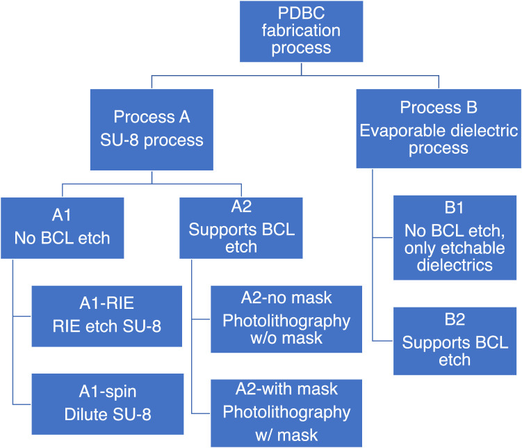
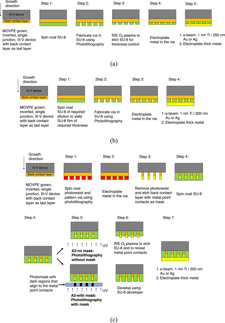
The patterned dielectric back contact (PDBC) structure can be used to form a point-contact architecture that features a dielectric spacer with spatially distributed, reduced-area metal point contacts between the semiconductor back not recognized contact layer and the metal back contact. In this structure, the dielectric-metal region provides higher reflectance and is electrically insulating. Reduced-area metal point contacts provide electrical conduction for the back contact but typically have lower reflectance. The fabrication methods discussed in this article were developed for thermophotovoltaic cells, but they apply to any III-V optoelectronic device requiring the use of a conductive and highly reflective back contact. Patterned dielectric back contacts may be used for enhanced sub-bandgap reflectance, for enhanced photon recycling near the bandgap energy, or both depending on the optoelectronic application. The following fabrication methods are discussed in the article•PDBC fabrication procedures for spin-on dielectrics and commonly evaporated dielectrics to form the spacer layer.•Methods to selectively etch a parasitically absorbing back contact layer using metal point contacts as an etch mask.•Methods incorporating a dielectric etch through different process techniques such as reactive ion and wet etching.
Keywords: Dielectrics; High-reflectivity mirror; Optoelectronics; Photovoltaics; SU-8; Via contacts.
© 2022 The Author(s).
Figures
References
-
- Arulanandam M.K., Steiner M.A., Tervo E.J., Young A.R., Kuritzky L.Y., Perl E.E., Narayan T.C., Kayes B.M., Briggs J.A., King R.R. GaAs thermophotovoltaic patterned dielectric back contact devices with improved sub-bandgap reflectance. Sol. Energy Mater. Sol. Cells. 2022;238
-
- Micha D.N., Höhn O., Oliva E., Klinger V., Bett A.W., Dimroth F. Development of back side technology for light trapping and photon recycling in GaAs solar cells. Prog. Photovolt. Res. Appl. 2019;27(2):163–170.
-
- Helmers H., Lopez E., Höhn O., Lackner D., Schön J., Schauerte M., Schachtner M., Dimroth F., Bett A.W. 68.9% efficient gaas-based photonic power conversion enabled by photon recycling and optical resonance. Phys. Status Solidi Rapid Res. Lett. 2021
-
- Gruginskie N., Cappelluti F., Bauhuis G., Tibaldi A., Giliberti G., Mulder P., Vlieg E., Schermer J. Limiting mechanisms for photon recycling in thin-film GaAs solar cells. Prog. Photovoltaics Res. Appl. 2021;29(3):379–390.
-
- Green M.A., Zhao J., Wang A., Reece P.J., Gal M. Efficient silicon light-emitting diodes. Nature. 2001;412(6849):805–808. - PubMed
LinkOut - more resources
Full Text Sources