. 2022 Nov 15;15(22):8091.
doi: 10.3390/ma15228091.

Ag-Decorated Si Microspheres Produced by Laser Ablation in Liquid: All-in-One Temperature-Feedback SERS-Based Platform for Nanosensing

Affiliations

Ag-Decorated Si Microspheres Produced by Laser Ablation in Liquid: All-in-One Temperature-Feedback SERS-Based Platform for Nanosensing

Stanislav Gurbatov et al. Materials (Basel). .

Abstract

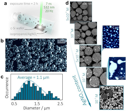
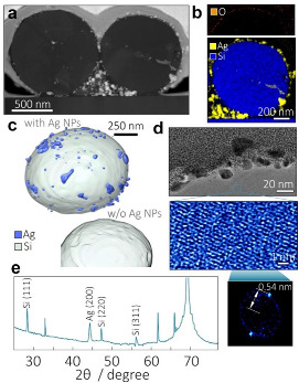
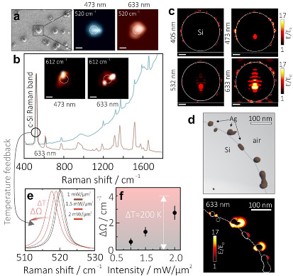
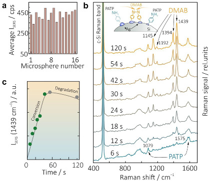
Combination of dissimilar materials such as noble metals and common semiconductors within unified nanomaterials holds promise for optoelectronics, catalysis and optical sensing. Meanwhile, difficulty of obtaining such hybrid nanomaterials using common lithography-based techniques stimulates an active search for advanced, inexpensive, and straightforward fabrication methods. Here, we report one-pot one-step synthesis of Ag-decorated Si microspheres via nanosecond laser ablation of monocrystalline silicon in isopropanol containing AgNO3. Laser ablation of bulk silicon creates the suspension of the Si microspheres that host further preferential growth of Ag nanoclusters on their surface upon thermal-induced decomposition of AgNO3 species by subsequently incident laser pulses. The amount of the AgNO3 in the working solution controls the density, morphology, and arrangement of the Ag nanoclusters allowing them to achieve strong and uniform decoration of the Si microsphere surface. Such unique morphology makes Ag-decorated Si microspheres promising for molecular identification based on the surface-enhanced Raman scattering (SERS) effect. In particular, the designed single-particles sensing platform was shown to offer temperature-feedback modality as well as SERS signal enhancement up to 106, allowing reliable detection of the adsorbed molecules and tracing their plasmon-driven catalytic transformations. Considering the ability to control the decoration degree of Si microspheres by Ag nanoclusters via amount of the AgNO3, the developed one-pot easy-to-implement PLAL synthesis holds promise for gram-scale production of high-quality hybrid nanomaterial for various nanophotonics and sensing applications.

Keywords: SERS; hybrid nanomaterials; plasmonics; pulsed laser ablation in liquid; silicon; silver.


Conflict of interest statement

The authors declare no conflict of interest.

Figures

Figure 1
Figure 1
(a) Schematic of the PLAL synthesis of Ag-Si microspheres upon ns-laser ablation of the monocrystalline Si wafer placed in the isopropanol containing AgNO3. (b) Top-view SEM image of the as-synthesized Ag-Si product dried on a Si wafer. (c) Size distribution of the Ag-Si microspheres. (d) Series of SEM images illustrating evolution of the density and geometry of the Ag nanoclusters on the surface of Si microspheres upon increase of the AgNO3 content in the working solution from 5 × 10⁻⁵ to 10−2 M.
Figure 2
Figure 2
(a) STEM image of the cross-sectional central cut made through the 1.1-µm diameter Ag-Si microspheres; (b) EDX composition mapping of the right-most Ag-Si microsphere showing distribution of Ag and Si elements as well as an oxide shell (top panel); (c) 3D model of the isolated Ag-Si microsphere made through SEM tomographic reconstruction from the series of multiple images of cross-sectional cuts. Bottom panel shows the same model where Ag nanoclusters were removed to illustrate crater-like Si surface morphology; (d) TEM image of the Ag-Si microsphere surface (top panel) as well as HR-TEM image and its FFT showing crystalline structure of the Si core (bottom panel); (e) XRD pattern of the Ag-Si nanopowder. All unmarked peaks represent contribution from the underlying Si substrate.
Figure 3
Figure 3
(a) Reference SEM image of the Ag-Si microspheres drop-casted onto the Si wafer as well as Raman images (at 520 ± 2 cm−1) of the chosen isolated nanoparticle at 473 and 633 nm laser pump wavelengths. (b) Representative averaged SERS spectra of the R6G capping the same Ag-Si microsphere at 473 and 633 nm laser pump wavelengths. Top insets show the distribution of the SERS signal (at 612 ± 2 cm−1) near the microsphere. (c) Normalized electric-field amplitude E/E0 near the isolated Ag-Si microsphere on the Ag mirror upon its excitation with a linearly polarized plane wave at 405, 473, 532, and 633 nm. (d) Close-up distribution of E/E0 near the isolated Ag nanoclusters on the Si surface at 633 nm pump as well as corresponding fragment of the 3D tomographic model of the Ag-Si microsphere used for modeling. (e) Shift of the detected c-Si Raman band at 520 cm−1 upon increasing the laser pump intensity (633 nm) of the Ag-Si microsphere from 0.5 to 2 mW/µm2. (f) Thermally induced shift of the c-Si band ΔΩ as a function of laser pump intensity.
Figure 4
Figure 4
(a) R6G SERS yield (intensity of the bands at 612 and 1652 cm−1) statistically averaged over measurements from 16 randomly chosen isolated Ag-Si microspheres produced at AgNO3 concentrations of 5 × 10⁻⁴ M. (b) Series of time-resolved SERS spectra of the PATP capping the isolated Ag-Si microsphere. Total laser exposure time ranging from 6 to 120 s is indicated near each spectrum. (c) Evolution of the intensity of the characteristics DMAB-related Raman band at 1439 cm−1 as a function of laser exposure time indicating PATP-to-DMAB conversion dynamics.

References

    1. Maier S.A. Plasmonics: Fundamentals and Applications. Volume 1. Springer; New York, NY, USA: 2007. p. 245.
    1. Kuznetsov A.I., Miroshnichenko A.E., Brongersma M.L., Kivshar Y.S., Luk’yanchuk B. Optically resonant dielectric nanostructures. Science. 2016;354:aag2472. doi: 10.1126/science.aag2472. - DOI - PubMed
    1. Jiang R., Li B., Fang C., Wang J. Metal/semiconductor hybrid nanostructures for plasmon-enhanced applications. Adv. Mater. 2014;26:5274–5309. doi: 10.1002/adma.201400203. - DOI - PubMed
    1. Fusco Z., Rahmani M., Tran-Phu T., Ricci C., Kiy A., Kluth P., Della Gaspera E., Motta N., Neshev D., Tricoli A.S.A. Photonic Fractal Metamaterials: A Metal–Semiconductor Platform with Enhanced Volatile-Compound Sensing Performance. Adv. Mater. 2020;32:2002471. doi: 10.1002/adma.202002471. - DOI - PubMed
    1. Atwater H.A., Polman A. Plasmonics for improved photovoltaic devices. Nat. Mater. 2010;9:205–213. doi: 10.1038/nmat2629. - DOI - PubMed

LinkOut - more resources