On-the-Fly Short-Pulse R2R Laser Patterning Processes for the Manufacturing of Fully Printed Semitransparent Organic Photovoltaics
- PMID: 36431703
- PMCID: PMC9692794
- DOI: 10.3390/ma15228218
On-the-Fly Short-Pulse R2R Laser Patterning Processes for the Manufacturing of Fully Printed Semitransparent Organic Photovoltaics
Abstract
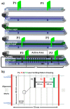
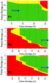
Ultrafast laser patterning is an essential technology for the low-cost and large area production of flexible Organic Electronic (OE) devices, such as Organic Photovoltaics (OPVs). In order to unleash the potential of ultrafast laser processing to perform the selective and high precision removal of complex multilayers from printed OPV stacks without affecting the underlying nanolayers, it is necessary to optimize its parameters for each nanolayer combination. In this work, we developed an efficient on-the-fly picosecond (ps) laser scribing process (P1, P2 and P3) using single wavelength and single step/pass for the precise and reliable in-line patterning of Roll-to-Roll (R2R) slot-die-coated nanolayers. We have investigated the effect of the key process parameters (pulse energy and overlap) on the patterning quality to obtain high selectivity on the ablation of each individual nanolayer. Finally, we present the implementation of the ultrafast laser patterning process in the manufacturing of fully R2R printed flexible semitransparent OPV modules with a 3.4% power conversion efficiency and 91% Geometric Fill Factor (GFF).
Keywords: fully printed; laser ablation; laser pattering; organic photovoltaics; roll-to-roll; semitransparent module.
Conflict of interest statement
The authors declare no conflict of interest.
Figures


References
-
- OE-A . White Paper OE-A Roadmap. 8th ed. VDMA Services GmbH; Frankfurt, Germany: 2020.
-
- Espinosa N., Lenzmann F.O., Ryley S., Angmo D., Hösel M., Søndergaard R.R., Huss D., Dafinger S., Gritsch S., Kroon J.M., et al. OPV for mobile applications: An evaluation of roll-to-roll processed indium and silver free polymer solar cells through analysis of life cycle, cost and layer quality using inline optical and functional inspection tools. J. Mater. Chem. A. 2013;1:6971–7278. doi: 10.1039/c3ta01611k. - DOI
-
- Gevorgyan S.A., Madsen M.V., Roth B., Corazza M., Hösel M., Søndergaard R.R., Jørgensen M., Krebs F.C. Lifetime of organic photovoltaics: Status and predictions. Adv. Energy Mater. 2016;6:1501208. doi: 10.1002/aenm.201501208. - DOI
-
- Kirchmeyer S. The OE-A roadmap for organic and printed electronics: Creating a guidepost to complex interlinked technologies, applications and markets. Transl. Mater. Res. 2016;3:010301. doi: 10.1088/2053-1613/3/1/010301. - DOI
-
- Krebs F.C. Fabrication and processing of polymer solar cells: A review of printing and coating techniques. Sol. Energy Mater. Sol. Cells. 2009;93:394–412. doi: 10.1016/j.solmat.2008.10.004. - DOI
Grants and funding
LinkOut - more resources
Full Text Sources

