Review
. 2022 Nov 23;8(11):1490-1505.
doi: 10.1021/acscentsci.2c01038. Epub 2022 Nov 1.

Controlled Preparation of Single-Walled Carbon Nanotubes as Materials for Electronics

Affiliations
Review

Controlled Preparation of Single-Walled Carbon Nanotubes as Materials for Electronics

Yuguang Chen et al. ACS Cent Sci. .

Abstract

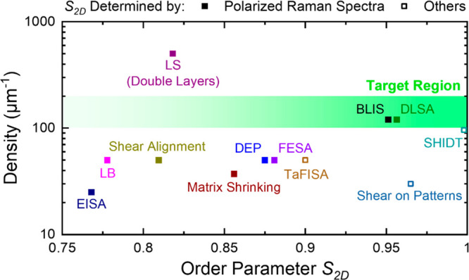
Single-walled carbon nanotubes (SWCNTs) are of particular interest as channel materials for field-effect transistors due to their unique structure and excellent properties. The controlled preparation of SWCNTs that meet the requirement of semiconducting and chiral purity, high density, and good alignment for high-performance electronics has become a key challenge in this field. In this Outlook, we outline the efforts in the preparation of SWCNTs for electronics from three main aspects, structure-controlled growth, selective sorting, and solution assembly, and discuss the remaining challenges and opportunities. We expect that this Outlook can provide some ideas for addressing the existing challenges and inspire the development of SWCNT-based high-performance electronics.


Conflict of interest statement

The authors declare no competing financial interest.

Figures

Figure 1
Figure 1
SWCNTs as materials for electronics. (a) False-colored scanning electron microscopy (SEM) images of an SWCNT-array-based ring oscillator with an inset schematic illustration of the gate structure. (b) Benchmarking of the stage delay of the champion SWCNT-array-based ring oscillators with state-of-the-art “0.18 μm” silicon devices. (a) and (b) are reproduced with permission from ref (32): copyright 2020, American Association for the Advancement of Science. (c) Image of the SWCNT-based modern microprocessor chip RV16X-NANO with SEM images of increasing magnifications exhibiting the layout of SWCNT FETs. Reproduced with permission from ref (33): copyright 2019, Springer Nature. (d) Progress on the purity and placement of SWCNTs in FETs summarized and predicted by Franklin in 2013. Reproduced with permission from ref (40): copyright 2013, Springer Nature. (e) Progress in improving the semiconducting purity of SWCNTs by controlled growth (blue squares) and sorting (red triangles). The larger icons show the milestones for fitting the trend lines.
Figure 2
Figure 2
Selective growth of s-SWCNTs. (a) Schematic of density of states of m- and s-SWCNTs. (b–d) Raman spectra (b) and atomic force microscopy (AFM) image (c) of SWCNT arrays grown from a mixed feedstock of methanol and ethanol and an SEM image of the FET devices (d) fabricated with those arrays. Reproduced from ref (49): copyright 2009, American Chemical Society. (e) Statistics of m-/s-SWCNTs grown from Fe/CeO2 and Fe/SiO2 catalysts. Reproduced from ref (56): copyright 2014, American Chemical Society. (f) Typical transport characteristics of the SWCNT-based FETs. The inset shows the statistical result of on–off ratios. Blue, green, orange, red represent results of SWCNTs grown with oxygen flow rates of 0, 0.1, 0.2, and 0.3 sccm, respectively. Reproduced from ref (51): copyright 2011, American Chemical Society. (g) Upper panel: Twisting the chirality of SWCNTs by reversing the electric field to induce renucleation. Lower panel: SEM image of the SWCNTs changing from metallic (bright ones) to semiconducting (dark ones). Reproduced with permission from ref (47): copyright 2018, Springer Nature.
Figure 3
Figure 3
Chirality-controlled growth of s-SWCNTs. (a) Abundances of different chiralities of (6,5)-enriched SWCNTs grown from CoMo catalyst. Reproduced from ref (60): copyright 2006, American Chemical Society. (b) Abundances of different chiralities of (9,8)-enriched SWCNTs grown from the sulfate-promoted Co/SiO2 catalyst. Reproduced from ref (63): copyright 2013, American Chemical Society. (c) Formation energy of SWCNTs with similar diameters on a WC (100) surface (inset: simulation result showing symmetrical matching of catalyst surface with tube ends). Reproduced with permission from ref (65): copyright 2017, Springer Nature. (d) Side views and top views of the interface between a (14,4) nanotube and the (1 0 10) plane of Co7W6 from DFT simulation results. (e) XRD patterns of the catalyst reduced by pure H2 (curve I, blue) and by H2/H2O (curve II, red), as well as the standard card of Co7W6 (black). The peak of (1 0 10) plane is highlighted. (f) Raman spectra (RBM region) of the (14,4)-enriched SWCNTs. (g) Abundance of (14,4) nanotubes and s-SWCNTs from a statistical analysis of Raman spectra after a water vapor treatment. (h, i) SEM images (h) and transport characteristics (i) of the FET devices fabricated with the (14,4)-enriched SWCNTs. (d–i) are reproduced from ref (46): copyright 2017 American Chemical Society.
Figure 4
Figure 4
Controlled growth of horizontally aligned SWCNT arrays. (a) Schematic of the “kite mechanism” for gas-flow-guided growth. Reproduced from ref (76): copyright 2007 American Chemical Society. (b) SEM image of the gas-flow-guided SWCNTs. Reproduced from ref (75): copyright 2004 American Chemical Society. (c, d) Hydromechanical simulation of streamline (c) and SEM image of the SWCNT arrays (d) when a cylindrical barrier was placed on the side of the substrate. Reproduced with permission from ref (78): copyright 2009 IOP Publishing. (e) SEM image of an aligned SWCNT array grown on sapphire substrate. Reproduced from ref (86): copyright 2008 American Chemical Society. (f) SEM image of aligned SWCNT arrays grown on a quartz substrate with patterned catalyst stripes. Reproduced with permission from ref (81): copyright 2007, Springer Nature. (g) Transmission electron microscopy (TEM) image of an SWCNT array with a density up to 160 tubes/μm. Reproduced with permission from ref (87): copyright 2015, Springer Nature. (h) Schematic of the thermocapillary purification process, where a thermocapillary resist is first deposited on the SWCNT array, then the m-SWCNTs are selectively exposed using Joule heat, and finally the m-SWCNTs are etched away and the thermocapillary resist is removed. Reproduced with permission from ref (84): copyright 2013, Springer Nature.
Figure 5
Figure 5
SWCNT sorting by SECP. (a, b) Molecular structure of PFO (a) and poly[9-(1-octylonoyl)-9H-carbazole-2,7-diyl] (PCz, b). (c) Radial view of molecular mechanics simulations of the wrapping conformation of a (15,0) PFO chain encased with six repeat units. (d) Absorbance spectra of CoMoCAT SWCNTs dispersed by SDBS in aqueous solution and PFO in toluene. (c) and (d) are reproduced with permission from ref (89): copyright 2007, Spinger Nature. (e) Schematic illustration of the solubilization of SWCNTs by coordination polymers composed of fluorene moieties and metal complexes (CP-M) and the removal of CP-M from SWCNT surface. Reproduced with permission from ref (105): copyright 2014, Spinger Nature. (f) Transfer characteristics of 1000 FETs. Reproduced with permission from ref (32): copyright 2020, American Association for the Advancement of Science.
Figure 6
Figure 6
SWCNT sorting by chromatography and DGU. (a) Absorption spectra of 12 kinds of single-chirality species separated by ion exchange chromatography. Reproduced with permission from ref (108): copyright 2009, Spinger Nature. (b) Schematic of the M/S and diameter separation by gel chromatography. Reproduced with permission from ref (112): copyright 2009, The Japan Society of Applied Physics. (c) Image of single-chirality species separated on a sub-millimeter scale by gel chromatography. Reproduced with permission from ref (117): copyright 2021, American Association for the Advancement of Science. (d) Photograph of the M/S separation of surfactant-dispersed SWCNTs by DGU. Reproduced with permission from ref (120): copyright 2006, Spinger Nature. (e) Photograph of HiPco SWCNTs sorted by nonlinear DGU. (f) Absorbance spectra of the layers marked in (e). (e) and (f )are reproduced with permission from ref (126): copyright 2010, Spinger Nature.
Figure 7
Figure 7
SWCNT sorting by ATPE. (a) Schematic of the oxidative extraction with sufficient oxidant added to fully oxidize SWCNTs and a photograph of the separated metallic SWCNTs and small-band-gap and large-band-gap SWCNTs. (b) Absorbance spectra of separated metallic SWCNTs and small-band-gap and large-band-gap SWCNTs. (a) and (b) are reproduced from ref (130): copyright 2015, American Chemical Society. (c) Absorption spectra of (13,7), (14,6), and (16,3) sorted by ATPE of alkane-filled SWCNTs. Reproduced from ref (132): copyright 2020, American Chemical Society. (d) Photograph of the single-chirality species sorted by ATPE of DNA-SWCNTs with the assistance of machine-learning-guided screening of DNA sequences. Reproduced from ref (134): copyright 2022, American Chemical Society. (e) Contour plot of the absorption spectra of each fraction obtained during the separation of TCT CCC TCT CCC TCT-SG65i. (f) Absorption spectra of (7,3), (6,5), (7,4), and (10,0) obtained from 2T, 6T, 10T and 13B fractions. (e) and (f) are reproduced from ref (136): Copyright 2019, American Chemical Society. (g) Schematic of the solvation energy spectrum.
Figure 8
Figure 8
Summary of the density and order parameter S2D of SWCNT arrays assembled by different solution methods. Abbreviations in the figure: BLIS, binary liquid interface-confined self-assembly; DEP, dielectrophoretic assembly; DLSA, dimension-limited self-alignment; EISA, evaporation-induced self-assembly; FESA, floating evaporative self-assembly; LB, Langmuir–Blodgett; LS, Langmuir–Schaefer; S2D, two-dimensional order parameter; SHIDT, spatially hindered integration based on DNA template; TaFISA, tangential flow interfacial self-assembly.
Figure 9
Figure 9
Methods for high-density assembly. (a) Schematic illustrations of the assembly process of the DLSA method. (b) SEM and cross-sectional TEM images of the assembled SWCNT arrays. (c) Benchmarking of peak transconductances versus gate lengths of the DLSA-based FETs with other reported SWCNT FETs and commercial silicon devices. (a)–(c) are reproduced with permission from ref (32): copyright 2020, American Association for the Advancement of Science. (d, e) Schematic illustrations, TEM images, and AFM images of the DNA nanotrenches before (d) and after (e) nanotube assembly in the SHIDT process. Reproduced with permission from ref (48): copyright 2020, American Association for the Advancement of Science.
Figure 10
Figure 10
Keys to reaching good alignment and high density of SWCNT arrays.

References

    1. Franklin A. D. Nanomaterials in Transistors: From High-Performance to Thin-Film Applications. Science 2015, 349, aab2750.10.1126/science.aab2750. - DOI - PubMed
    1. Wu Y.; Farmer D. B.; Xia F.; Avouris P. Graphene Electronics: Materials, Devices, and Circuits. Proc. IEEE 2013, 101 (7), 1620–1637. 10.1109/JPROC.2013.2260311. - DOI
    1. Li M.-Y.; Su S.-K.; Wong H.-S. P.; Li L.-J. How 2d Semiconductors Could Extend Moore’s Law. Nature 2019, 567, 169–170. 10.1038/d41586-019-00793-8. - DOI - PubMed
    1. del Alamo J. A. Nanometre-Scale Electronics with III-V Compound Semiconductors. Nature 2011, 479 (7373), 317–323. 10.1038/nature10677. - DOI - PubMed
    1. International Technology Roadmap for Semiconductors. https://www.semiconductors.org/resources/2013-international-technology-r... (accessed September 3, 2022).