. 2022 Dec 5;13(1):7491.
doi: 10.1038/s41467-022-35229-x.

High-throughput screening of 2D van der Waals crystals with plastic deformability

Affiliations

High-throughput screening of 2D van der Waals crystals with plastic deformability

Zhiqiang Gao et al. Nat Commun. .

Abstract

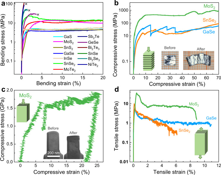
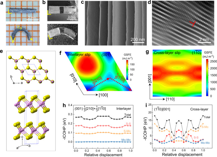
Inorganic semiconductors exhibit multifarious physical properties, but they are prevailingly brittle, impeding their application in flexible and hetero-shaped electronics. The exceptional plasticity discovered in InSe crystal indicates the existence of abundant plastically deformable two-dimensional van der Waals (2D vdW) materials, but the conventional trial-and-error method is too time-consuming and costly. Here we report on the discovery of tens of potential 2D chalcogenide crystals with plastic deformability using a nearly automated and efficient high-throughput screening methodology. Seven candidates e.g., famous MoS2, GaSe, and SnSe2 2D materials are carefully verified to show largely anisotropic plastic deformations, which are contributed by both interlayer and cross-layer slips involving continuous breaking and reconstruction of chemical interactions. The plasticity becomes a new facet of 2D materials for deformable or flexible electronics.


Conflict of interest statement

The authors declare no competing interests.

Figures

Fig. 1
Fig. 1. High-throughput methodology to screen 2D vdW chalcogenide crystals with plastic deformability.
a High-throughput calculation flow. All the steps are automatized except for steps 6 and 15. b Crystal structure of CeTe3 as a case example. c GSFE surface of (001) plane (up) to analyze the interlayer slip (down) for CeTe3. The black dots represent slip vectors, corresponding to the various slipped structures. The GSFE surface can be divided into 16 equivalent triangles (see black dash lines) because of the crystal symmetry. d Three possible cross-layer cleavage planes for CeTe3.
Fig. 2
Fig. 2. Plastically deformable 2D vdW chalcogenide crystals discovered by high-throughput screening.
a Schematics of the plastic (up) and brittle (down) bending deformations. The interlayer/cross-layer slips and/or cleavages are highlighted. b Ec,inter × Ec,cross vs. Eb,inter for 2D vdW crystals. Each point represents a 2D vdW material with the detailed data shown in Supplementary Table 1. The plastic and brittle crystals verified in experiment are marked by red and blue dots, respectively. c Photos of bent plastic and brittle crystals with a bending radius of 1 mm. The smallest grid in the background denotes 1 mm.
Fig. 3
Fig. 3. Mechanical properties of selected 2D vdW crystals.
a Three-point bending stress-strain curves for the selected crystals. b Compressive stress-strain curves for MoS2, GaSe, and SnSe2 crystals. The inset photos show a MoS2 crystal before and after compression. c In situ compressive stress-strain curve of a MoS2 small pillar. The inset shows the specimen transmission electron microscopy (TEM) images before and after test. d Tensile stress-strain curves for MoS2, GaSe, and SnSe2 crystals.
Fig. 4
Fig. 4. Plasticity mechanism of MoS2.
a Optical images of a bar-shaped MoS2 crystal before and after bending. b Scanning electron microscopy (SEM) images of an Ag bar before and after bending. Black ink is marked on sample’s top surface to help to fix the position. c SEM image of area 1 in a. d, Inverse Fourier transform of the dark-field scanning transmission electron microscopy (IFT-DF-STEM) image of area 2 in a. e Crystal structure of 2H-MoS2. f Generalized stacking fault energy (GSFE) surface of MoS2 (001) plane. g GSFE surface of MoS2 (11¯0) plane. h The integrated crystal orbital Hamilton population (-ICOHP) analysis of the interlayer chemical interactions between the slip planes for (001)1/3[210]+1/3[11¯0] slip system shown in f. i -ICOHP analysis of the chemical interactions between the slip planes for (11¯0)[001] slip system shown in g.

References

    1. Seeger, K. Semiconductor Physics. (Springer Science & Business Media, 2013).
    1. Guruswamy, S., Faber, K. T. & Hirth, J. P. In The Mechanical Properties of Semiconductors Vol. 37 Semiconductors and Semimetals (eds Katherine T. Faber & Kevin J. Malloy) 189–230 (Elsevier, 1992).
    1. Kim DH, et al. Stretchable and foldable silicon integrated circuits. Science. 2008;320:507–511. doi: 10.1126/science.1154367. - DOI - PubMed
    1. Oh JY, et al. Intrinsically stretchable and healable semiconducting polymer for organic transistors. Nature. 2016;539:411–415. doi: 10.1038/nature20102. - DOI - PubMed
    1. Shi X, et al. Room-temperature ductile inorganic semiconductor. Nat. Mater. 2018;17:421–426. doi: 10.1038/s41563-018-0047-z. - DOI - PubMed