. 2022 Dec 9;8(49):eabq8246.
doi: 10.1126/sciadv.abq8246. Epub 2022 Dec 9.

Chirality logic gates

Affiliations

Chirality logic gates

Yi Zhang et al. Sci Adv. .

Abstract

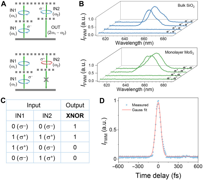
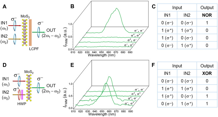
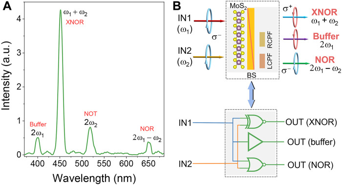
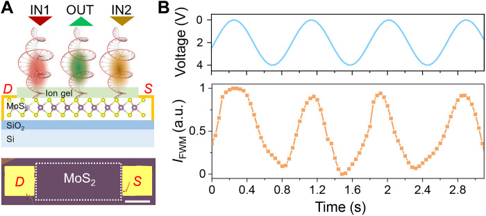
The ever-growing demand for faster and more efficient data transfer and processing has brought optical computation strategies to the forefront of research in next-generation computing. Here, we report a universal computing approach with the chirality degree of freedom. By exploiting the crystal symmetry-enabled well-known chiral selection rules, we demonstrate the viability of the concept in bulk silica crystals and atomically thin semiconductors and create ultrafast (<100-fs) all-optical chirality logic gates (XNOR, NOR, AND, XOR, OR, and NAND) and a half adder. We also validate the unique advantages of chirality gates by realizing multiple gates with simultaneous operation in a single device and electrical control. Our first demonstrations of logic gates using chiral selection rules suggest that optical chirality could provide a powerful degree of freedom for future optical computing.


Figures

Fig. 1.
Fig. 1.. Illustration of the chirality logic gate and its concept universality in the selection of materials and optical processes.
The generated output signal (i.e., OUT) in a nonlinear optical process is determined by the chirality of the two input beams (i.e., IN1 and IN2). The top right inset shows a top view of monolayer MoS2 and bulk SiO2 with threefold rotational symmetry to indicate the concept universality in the material selection. The bottom left inset presents the concept universality in the selection of nonlinear optical processes. IN and OUT denote the input and output beams, respectively.
Fig. 2.
Fig. 2.. Chirality XNOR logic gate.
(A) The optical chirality–dependent selection rule in FWM due to threefold rotational symmetry in materials. (B) The normalized FWM output spectra in bulk SiO2 and monolayer MoS2 under the excitation of two input beams with different chirality combinations. (C) The truth table of the chirality XNOR logic gate. (D) The normalized cross-correlation spectrum of the FWM signal in MoS2 with a Gauss fit. a.u., arbitrary units.
Fig. 3.
Fig. 3.. Diversity of chirality logic gates.
(A) Schematic illustration of NOR gate. (B) Output FWM spectra behind LCPF. (C) Truth table of NOR chirality logic gate. (D) Schematic illustration of XOR gate. (E) Output FWM spectra after the insertion of the half–wave plate in input beam 2. (F) Truth table of XOR chirality logic gate. The similar concept applies to bulk SiO2.
Fig. 4.
Fig. 4.. Simultaneous construction of multiple chirality logic gates.
(A) Simultaneous observation of SHG, SFG, and FWM spectra and their corresponding chirality logic gates. The two input beams are ω1 (~800 nm) and ω2 (~1036 nm) with σ polarization. (B) The simplified schematic illustration of the logic gates by inserting a beam splitter (BS) and different filters after monolayer MoS2 (top) and its equivalent logic gate network (bottom).
Fig. 5.
Fig. 5.. Proof-of-concept demonstration of electrically controllable chirality logic gate.
(A) Schematic of the chirality logic gate based on a MoS2 field-effect transistor with two σ+ circularly polarized incident beams (top) and one σ+ circularly polarized output beam, where S, D, and G denote the source, drain, and gate electrodes, respectively. The ion gel acts as the gate dielectric between the gate and source electrodes. Bottom denotes the optical image of the monolayer MoS2 channel (white rectangle) with source-drain contacts on the SiO2 substrate. Scale bar, 250 μm. (B) The modulated peak intensity of FWM (orange curve) under the gate voltage (blue curve). The two input beams are ~800 and 1036 nm with σ+ polarization. The results are rescaled through min-max normalization.

References

    1. W. Liu, M. Li, R. S. Guzzon, E. J. Norberg, J. S. Parker, M. Lu, L. A. Coldren, J. Yao,A fully reconfigurable photonic integrated signal processor. Nat. Photon. 10,190–195 (2016).
    1. E. N. Mohammadi, B. Edwards, N. Engheta,Inverse-designed metastructures that solve equations. Science 363,1333–1338 (2019). - PubMed
    1. D. Perez-Lopez, A. Lopez, P. DasMahapatra, J. Capmany,Multipurpose self-configuration of programmable photonic circuits. Nat. Commun. 11,6359 (2020). - PMC - PubMed
    1. H. Yang, V. Khayrudinov, V. Dhaka, H. Jiang, A. Autere, H. Lipsanen, Z. Sun, H. Jussila,Nanowire network–based multifunctional all-optical logic gates. Sci. Adv. 4,eaar7954 (2018). - PMC - PubMed
    1. P. Singh, D. K. Tripathi, S. Jaiswal, H. K. Dixit,All-optical logic gates: Designs, classification, and comparison. Adv. Opt. Technol. 2014,275083 (2014).

LinkOut - more resources