

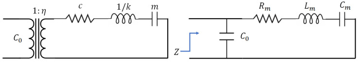
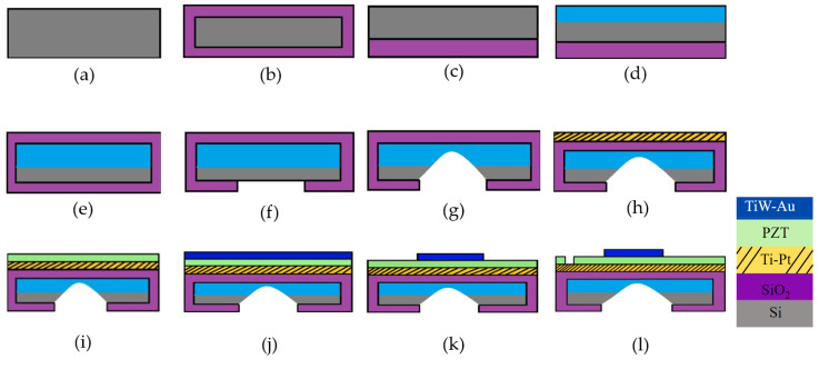
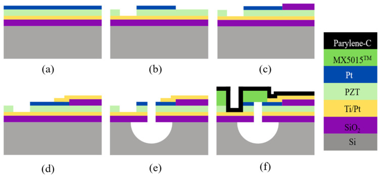
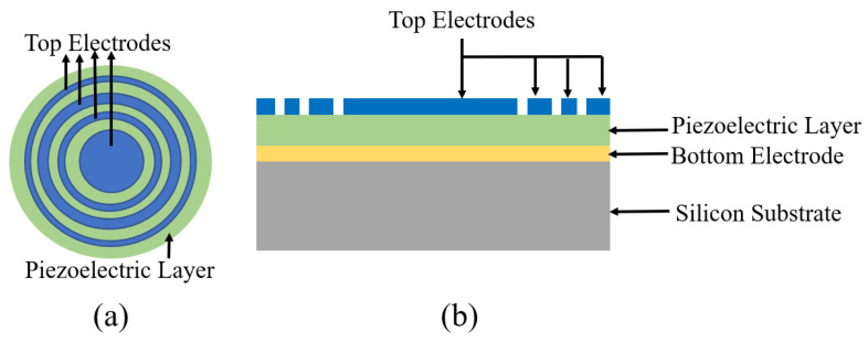
Piezoelectric Micromachined Ultrasonic Transducers (PMUTs): Performance Metrics, Advancements, and Applications
- PMID: 36501852
- PMCID: PMC9738559
- DOI: 10.3390/s22239151
Piezoelectric Micromachined Ultrasonic Transducers (PMUTs): Performance Metrics, Advancements, and Applications
Abstract
With the development of technology, systems gravitate towards increasing in their complexity, miniaturization, and level of automation. Amongst these systems, ultrasonic devices have adhered to this trend of advancement. Ultrasonic systems require transducers to generate and sense ultrasonic signals. These transducers heavily impact the system's performance. Advancements in microelectromechanical systems have led to the development of micromachined ultrasonic transducers (MUTs), which are utilized in miniaturized ultrasound systems. Piezoelectric micromachined ultrasonic transducers (PMUTs) exhibit higher capacitance and lower electrical impedance, which enhances the transducer's sensitivity by minimizing the effect of parasitic capacitance and facilitating their integration with low-voltage electronics. PMUTs utilize high-yield batch microfabrication with the use of thin piezoelectric films. The deposition of thin piezoelectric material compatible with complementary metal-oxide semiconductors (CMOS) has opened novel avenues for the development of miniaturized compact systems with the same substrate for application and control electronics. PMUTs offer a wide variety of applications, including medical imaging, fingerprint sensing, range-finding, energy harvesting, and intrabody and underwater communication links. This paper reviews the current research and recent advancements on PMUTs and their applications. This paper investigates in detail the important transduction metrics and critical design parameters for high-performance PMUTs. Piezoelectric materials and microfabrication processes utilized to manufacture PMUTs are discussed. Promising PMUT applications and outlook on future advancements are presented.
Keywords: CMOS integration; acoustic pressure; acoustic sensing; bandwidth; electromechanical coupling; microelectromechanical systems; microfabrication; micromachined ultrasonic transducers; pulse-echo imaging; resonant frequency.
Conflict of interest statement
The authors declare no conflict of interest.
Figures
References
-
- Lethiecq M., Levassort F., Certon D., Tran-Huu-Hue L.P. Piezoelectric and Acoustic Materials for Transducer Applications. Springer; Berlin/Heidelberg, Germany: 2008. Piezoelectric Transducer Design for Medical Diagnosis and NDE.
-
- Akasheh F., Myers T., Fraser J.D., Bose S., Bandyopadhyay A. Development of Piezoelectric Micromachined Ultrasonic Transducers. Sens. Actuators A Phys. 2004;111:275–287. doi: 10.1016/j.sna.2003.11.022. - DOI
-
- Muralt P., Baborowski J. Micromachined Ultrasonic Transducers and Acoustic Sensors Based on Piezoelectric Thin Films. Volume 12 Kluwer Academic Publishers; Alphen aan den Rijn, The Netherlands: 2004.
Publication types
MeSH terms
LinkOut - more resources
Full Text Sources
Other Literature Sources
