. 2022 Dec 6;12(12):1132.
doi: 10.3390/bios12121132.

Stabilization of Copper-Based Biochips with Alumina for Biosensing Application

Affiliations

Stabilization of Copper-Based Biochips with Alumina for Biosensing Application

Nour Beydoun et al. Biosensors (Basel). .

Abstract

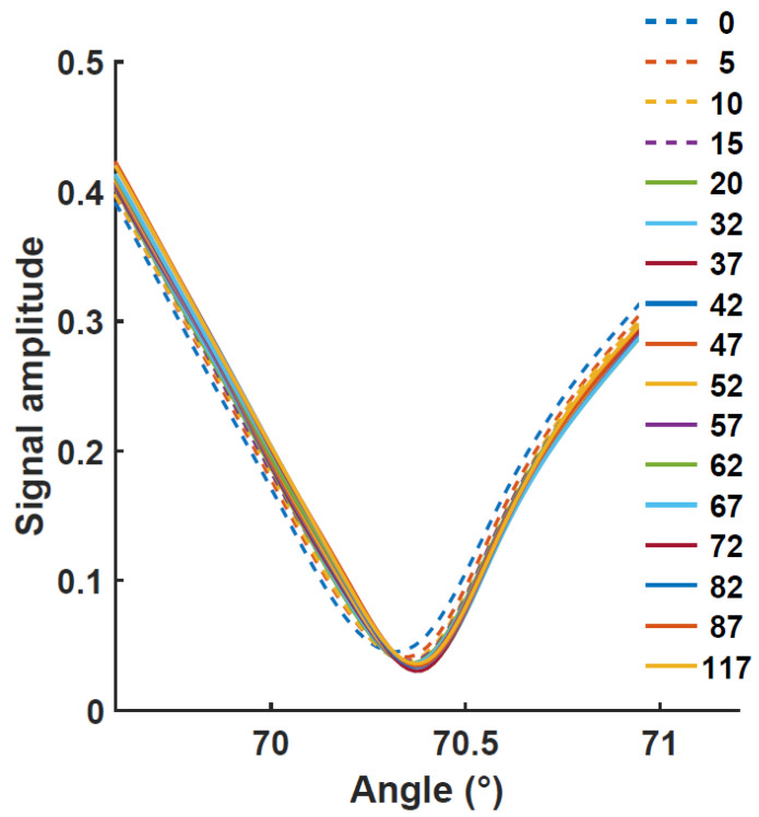
Surface plasmon resonance devices typically rely on the use of gold-coated surfaces, but the use of more abundant metals is desirable for the long-term development of plasmonic biochips. As a substitute for gold, thin copper films have been deposited on glass coverslips by thermal evaporation. As expected, these films immersed in a water solution initially exhibit an intense plasmonic resonance comparable to gold. However, without protection, an angle-resolved optical analysis shows a rapid degradation of the copper, characterized by a continuous angular shift of the plasmonic resonance curve. We show that copper films protected with a thin layer of aluminum oxide of a few nanometers can limit the oxidation rate for a sufficient time to perform some standard measurements. As the process is simple and compatible with the current biochip production technique, such an approach could pave the way for the production of alternative and more sustainable biochips.

Keywords: biochips; biosensors; copper; plasmonic; surface plasmon resonance.


Conflict of interest statement

The authors declare no conflict of interest.

Figures

Figure 1
Figure 1
Experimental and simulated UV-visible spectra showing simulated and experimental transmittance of the optical chip coated with about 46 nm of Cu (blue) and with the addition of about 3 nm of Al2O3 Cu (green).
Figure 2
Figure 2
(A) Scanning electron micrograph of copper thin film deposited at room temperature. (B) Scanning electron micrograph of copper thin film deposited at room temperature protected by 3 nm of Al2O3. (C) Atomic force micrograph of copper thin film deposited at room temperature. (D) Atomic force micrograph of copper thin film deposited at room temperature protected by Al2O3. An RMS topography value of 1.0 nm was obtained on the bare copper.
Figure 3
Figure 3
SPR curves for bare Cu thin films deposited on glass (46 nm) being in contact with deionized water. The time indicated in the legend is in minutes. The minimum amplitude is about 0.13 corresponding to a reflectivity of less than 2%.
Figure 4
Figure 4
(a) Time evolution of the resonant angle for (a) the bare Cu thin film on glass and (b) the Cu thin film protected with 3nm of oxide, (b) Evolution of the CuO oxide growth at the bare Cu surface (in blue) and the corresponding reduction of the Cu metal (green) determined from the resonant angle change.
Figure 5
Figure 5
SPR curves in PBS solution for the Al2O3 protected copper for different time variations for the position of the minimum angle versus time for Cu thin films deposited on glass (46 nm) covered by 2 to 3 nm of Al2O3 being in contact with a PBS buffer electrolyte. The time is given in minutes in the legend.
Figure 6
Figure 6
SPR curves for protected Cu thin films in contact with 20 mM PBS. The glass coverslide was coated with 46 nm of copper and protected with about 2 nm of Al2O3. The alumina surface was exposed to an oxygen plasma treatment of 12 min. After 250 min in the solution, an angle shift started to appear (dashed lines). The time is given in minutes in the legend.
Figure 7
Figure 7
SPR curves for Cu thin films deposited on glass (46 nm) protected by 5 nm Al2O3 being in contact with 20 mM PBS. The time is given in minutes in the legend.
Figure 8
Figure 8
Simulation realized at 680 nm using the Fresnel coefficient for p-polarized light. (a) Simulation of an oxidized Cu 46 nm surface, for each 1 nm of CuO there is 0.563 nm of Cu removed. (b) Simulation of a 46 nm Cu surface passivated with different Al2O3 thickness. A simulation of a 47 nm Au surface with 2 nm of Cr adhesion layer is presented as a matter of comparison. The copper oxide growth in Figure 4b is interpolated from the position of the resonance given in this figure.

References

    1. Qu J.-H., Dillen A., Saeys W., Lammertyn J., Spasic D. Advancements in SPR biosensing technology: An overview of recent trends in smart layers design, multiplexing concepts, continuous monitoring and in vivo sensing. Anal. Chim. Acta. 2020;1104:10–27. doi: 10.1016/j.aca.2019.12.067. - DOI - PubMed
    1. Hagelüken C. Recycling of (critical) metals. Crit. Met. Handb. 2014:41–69. doi: 10.1002/9781118755341.ch3. - DOI
    1. Li L., Liu G., Pan D., Wang W., Wu Y., Zuo T. Overview of the recycling technology for copper-containing cables. Resour. Conserv. Recycl. 2017;126:132–140. doi: 10.1016/j.resconrec.2017.07.024. - DOI
    1. Figueiredo V., Elangovan E., Gonçalves G., Barquinha P., Pereira L., Franco N., Alves E., Martins R., Fortunato E. Effect of post-annealing on the properties of copper oxide thin films obtained from the oxidation of evaporated metallic copper. Appl. Surf. Sci. 2008;254:3949–3954. doi: 10.1016/j.apsusc.2007.12.019. - DOI
    1. Maeda Y., Akita T., Kohyama M. High Activity of Gold/Tin-Dioxide Catalysts for Low-Temperature CO Oxidation: Application of a Reducible Metal Oxide to a Catalyst Support. Catal. Lett. 2014;144:2086–2090. doi: 10.1007/s10562-014-1376-4. - DOI