Hyperchaos, Intermittency, Noise and Disorder in Modified Semiconductor Superlattices
- PMID: 36554107
- PMCID: PMC9777605
- DOI: 10.3390/e24121702
Hyperchaos, Intermittency, Noise and Disorder in Modified Semiconductor Superlattices
Abstract
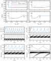
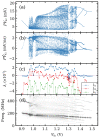
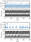
Weakly coupled semiconductor superlattices under DC voltage bias are nonlinear systems with many degrees of freedom whose nonlinearity is due to sequential tunneling of electrons. They may exhibit spontaneous chaos at room temperature and act as fast physical random number generator devices. Here we present a general sequential transport model with different voltage drops at quantum wells and barriers that includes noise and fluctuations due to the superlattice epitaxial growth. Excitability and oscillations of the current in superlattices with identical periods are due to nucleation and motion of charge dipole waves that form at the emitter contact when the current drops below a critical value. Insertion of wider wells increases superlattice excitability by allowing wave nucleation at the modified wells and more complex dynamics. Then hyperchaos and different types of intermittent chaos are possible on extended DC voltage ranges. Intrinsic shot and thermal noises and external noises produce minor effects on chaotic attractors. However, random disorder due to growth fluctuations may suppress any regular or chaotic current oscillations. Numerical simulations show that more than 70% of samples remain chaotic when the standard deviation of their fluctuations due to epitaxial growth is below 0.024 nm (10% of a single monolayer) whereas for 0.015 nm disorder suppresses chaos.
Keywords: chaos; chaos design; chaotic devices; fast true random number generators; fluctuations; hyperchaos; intermittency; nonlinear electron transport; secure communications; semiconductor superlattices.
Conflict of interest statement
The authors declare no conflict of interest.
Figures


Similar articles
-
Nonlinear Charge Transport and Excitable Phenomena in Semiconductor Superlattices.Entropy (Basel). 2024 Aug 8;26(8):672. doi: 10.3390/e26080672. Entropy (Basel). 2024. PMID: 39202142 Free PMC article. Review.
-
Designing Hyperchaos and Intermittency in Semiconductor Superlattices.Phys Rev Lett. 2021 Aug 27;127(9):096601. doi: 10.1103/PhysRevLett.127.096601. Phys Rev Lett. 2021. PMID: 34506173
-
Noise-enhanced chaos in a weakly coupled GaAs/(Al,Ga)As superlattice.Phys Rev E. 2017 Jan;95(1-1):012218. doi: 10.1103/PhysRevE.95.012218. Epub 2017 Jan 30. Phys Rev E. 2017. PMID: 28208354
-
Coherence Resonance and Stochastic Resonance in an Excitable Semiconductor Superlattice.Phys Rev Lett. 2018 Aug 24;121(8):086805. doi: 10.1103/PhysRevLett.121.086805. Phys Rev Lett. 2018. PMID: 30192625
-
Is there chaos in the brain? II. Experimental evidence and related models.C R Biol. 2003 Sep;326(9):787-840. doi: 10.1016/j.crvi.2003.09.011. C R Biol. 2003. PMID: 14694754 Review.
Cited by
-
Nonlinear Charge Transport and Excitable Phenomena in Semiconductor Superlattices.Entropy (Basel). 2024 Aug 8;26(8):672. doi: 10.3390/e26080672. Entropy (Basel). 2024. PMID: 39202142 Free PMC article. Review.
References
-
- Esaki L., Tsu R. Superlattice and Negative Differential Conductivity in Semiconductors. IBM J. Res. Dev. 1970;14:61–65. doi: 10.1147/rd.141.0061. - DOI
-
- Esaki L., Chang L.L. New Transport Phenomenon in a Semiconductor “Superlattice”. Phys. Rev. Lett. 1974;33:495–498. doi: 10.1103/PhysRevLett.33.495. - DOI
-
- Allan G., Bastard G., Boccara N., Lannoo M., Voos M., editors. Heterojunctions and Semiconductor Superlattices. Springer; Berlin/Heidelberg, Germany: 1986.
-
- Grahn H.T., editor. Semiconductor Superlattices. Growth and Electronic Properties. World Scientific; Singapore: 1995.
-
- Bonilla L.L., Grahn H.T. Non-linear dynamics of semiconductor superlattices. Rep. Prog. Phys. 2005;68:577–683. doi: 10.1088/0034-4885/68/3/R03. - DOI
Grants and funding
LinkOut - more resources
Full Text Sources

