. 2022 Dec 24;11(1):347.
doi: 10.1038/s41377-022-01058-2.

Planarized THz quantum cascade lasers for broadband coherent photonics

Affiliations

Planarized THz quantum cascade lasers for broadband coherent photonics

Urban Senica et al. Light Sci Appl. .

Erratum in

Abstract

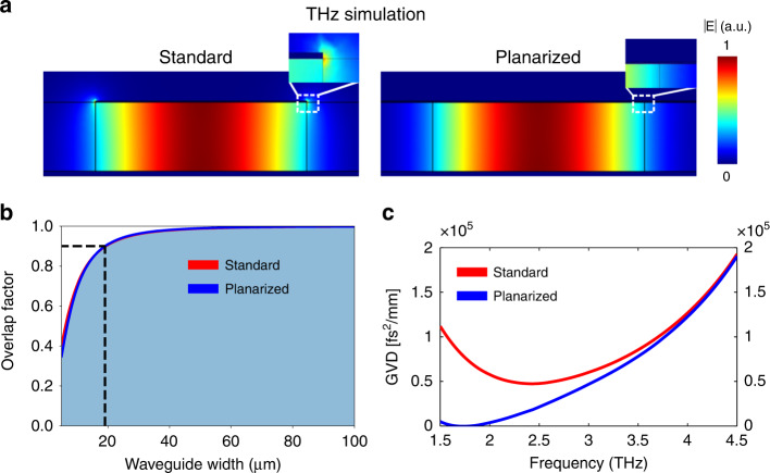
Recently, there has been a growing interest in integrated THz photonics for various applications in communications, spectroscopy and sensing. We present a new integrated photonic platform based on active and passive elements integrated in a double-metal, high-confinement waveguide layout planarized with a low-loss polymer. An extended top metallization keeps waveguide losses low while improving dispersion, thermal and RF properties, as it enables to decouple the design of THz and microwave cavities. Free-running on-chip quantum cascade laser combs spanning 800 GHz, harmonic states with over 1.1 THz bandwidth and RF-injected broadband incoherent states spanning over nearly 1.6 THz are observed using a homogeneous quantum-cascade active core. With a strong external RF drive, actively mode-locked pulses as short as 4.4 ps can be produced, as measured by SWIFTS. We demonstrate as well passive waveguides with low insertion loss, enabling the tuning of the laser cavity boundary conditions and the co-integration of active and passive elements on the same THz photonic chip.


Conflict of interest statement

The authors declare no competing interests.

Figures

Fig. 1
Fig. 1. Our new platform for broadband coherent THz photonics is based on planarized active and passive waveguides embedded in BCB, a low-loss polymer.
I. The planarized active waveguide consists of a standard double metal waveguide encompassed in BCB and an extended top contact metallization, which enables narrower active ridge geometries and the placement of bonding wires over the passive section. This configuration preserves the low waveguide losses of double metal waveguides while improving the dispersion, RF and thermal properties (see text for details). II. Passive waveguides can also be fabricated, consisting of metallic stripes on top of BCB, which provide confinement and guide the optical mode. These can be used to co-integrate active and passive elements on the same chip
Fig. 2
Fig. 2. Numerical simulation results with a comparison of standard and planarized waveguide properties at typical THz QCL frequencies.
a COMSOL 2D eigenmode simulation of a 40 μm wide waveguide at 3 THz. While there are field spikes present in the standard waveguide at the corners, for planarized waveguides the field distribution is smooth also at the environment boundary. b Computed overlap factors with the active region are comparable for the standard and planarized waveguides. The dashed line indicates the width where the overlap factor drops below 90%, for a frequency of 3 THz. c Computed chromatic dispersion for a waveguide width of 40 μm. At low frequencies (3 THz and below), the planarized waveguide has a significantly lower GVD than a standard waveguide
Fig. 3
Fig. 3. Optimized sample mounting and simulated RF properties of planarized waveguides.
a Illustration of the sample mounting with a custom RF-optimized PCB. Several short signal wires are connected from a 50 Ω matched coplanar waveguide to one end of the waveguide, with short ground wires for minimal RF injection and readout losses (inset, top left). The DC laser bias is provided through a separate contact pad (inset, top right). b 2D and 3D eigenmode numerical simulations of the RF field at 20 GHz show that the whole extended top metallization encompasses a cavity with the ground plane. c Computed impedance from 2D COMSOL simulations for a frequency of 20 GHz and a varying active waveguide width. Typical waveguide widths are marked with circles
Fig. 4
Fig. 4. Measurement results of a planarized ridge waveguide device.
a SEM image of a planarized, 40 μm wide ridge waveguide device, showing the cleaved front facet. The bonding wires are placed on the extended top metallization over the BCB-covered area. b LIV curves of a ridge laser sample measured in pulsed mode (500 ns pulses, 10% duty cycle) and in CW at a heatsink temperature of 40 K. c A free-running frequency comb spanning around 800 GHz, with the measured single strong RF beatnote (−55 dBm) shown in the inset. d A broadband free-running third harmonic state, covering a bandwidth of 1.1 THz. e With strong RF injection (+32 dBm at source) close to the free-running mode spacing, the emission spectrum can be broadened, spanning around 1.5 THz
Fig. 5
Fig. 5. SWIFT Spectroscopy on a planarized ridge device with different RF injection powers.
a Schematic of the SWIFTS setup, featuring an FTIR and a hot electron bolometer (HEB) as a fast detector. b, c Measurements of a weakly-injected free-running ridge device show relatively flat intermodal phase differences in two main groups, and the reconstructed time profile has a strongly amplitude-modulated periodic output intensity. d, e Strong RF injection (+32 dBm at the source) close to the repetition rate frequency on a ridge device close to lasing threshold results in active mode locking, producing pulses as short as 4.4 ps (close to the Fourier limit, dotted line). Here, the signal-to-noise ratio of the HEB measurement is reduced due to RF pickup problems with stronger RF injection
Fig. 6
Fig. 6. Simulation and measurement results of passive waveguides co-integrated with active planarized ridge devices.
a Optical microscope image of a ridge device co-integrated with straight and curved passive waveguide elements, consisting of a metallized stripe on top of BCB (width 60 μm, mini-mum bending radius R = 500 μm). Insets show the simulated THz wave propagation with minimal scattering and bending losses at 3 THz. b Simulated electric field distribution in the passive waveguide cross-section at 3 THz. In the case of a straight waveguide, the intensity is concentrated symmetrically below the metal stripe, while it shifts to the outer side in the case of a bent path. c False color SEM images of the cleaved passive waveguide with a flat BCB end facet. d Computed passive waveguide propagation losses in dB/mm for a varying bend radius, obtained by COMSOL 2D eigenmode simulations at a frequency of 3 THz. The total losses are split into contributions from absorption loss (overlap with lossy metals and BCB) and radiative loss (bending loss), which is negligible for bend radii above 230 μm. e The LIVs measured in pulsed (500 ns pulses, 10% duty cycle, 20 K) show an increased threshold current density and a higher slope efficiency, both consistent with the lower end facet reflectivity. f Spectrum of a free-running device (CW, T = 20 K) in the comb regime with a bandwidth over 1 THz and a single RF beatnote above −60 dBm, indicating that the reduced cavity feedback can be beneficial for comb formation

References

    1. Thomson D, et al. Roadmap on silicon photonics. J. Opt. 2016;18:073003. doi: 10.1088/2040-8978/18/7/073003. - DOI
    1. Schwarz B, et al. Monolithically integrated mid-infrared lab-on-a-chip using plasmonics and quantum cascade structures. Nat. Commun. 2014;5:4085. doi: 10.1038/ncomms5085. - DOI - PMC - PubMed
    1. Smit M, Williams K, van der Tol J. Past, present, and future of InP-based photonic integration. APL Photonics. 2019;4:050901. doi: 10.1063/1.5087862. - DOI
    1. Sengupta K, Nagatsuma T, Mittleman DM. Terahertz integrated electronic and hybrid electronic-photonic systems. Nat. Electron. 2018;1:622–635. doi: 10.1038/s41928-018-0173-2. - DOI
    1. Köhler R, et al. Terahertz semiconductor-heterostructure laser. Nature. 2002;417:156–159. doi: 10.1038/417156a. - DOI - PubMed