Review
. 2022 Dec 21;2(6):450-485.
doi: 10.1021/acsnanoscienceau.2c00017. Epub 2022 Sep 16.

Graphene and Beyond: Recent Advances in Two-Dimensional Materials Synthesis, Properties, and Devices

Affiliations
Review

Graphene and Beyond: Recent Advances in Two-Dimensional Materials Synthesis, Properties, and Devices

Yu Lei et al. ACS Nanosci Au. .

Abstract

Since the isolation of graphene in 2004, two-dimensional (2D) materials research has rapidly evolved into an entire subdiscipline in the physical sciences with a wide range of emergent applications. The unique 2D structure offers an open canvas to tailor and functionalize 2D materials through layer number, defects, morphology, moiré pattern, strain, and other control knobs. Through this review, we aim to highlight the most recent discoveries in the following topics: theory-guided synthesis for enhanced control of 2D morphologies, quality, yield, as well as insights toward novel 2D materials; defect engineering to control and understand the role of various defects, including in situ and ex situ methods; and properties and applications that are related to moiré engineering, strain engineering, and artificial intelligence. Finally, we also provide our perspective on the challenges and opportunities in this fascinating field.


Conflict of interest statement

The authors declare no competing financial interest.

Figures

Figure 1
Figure 1
Overview of the scope of this paper. Focusing on the recent advancements in the field of 2D materials, we discuss theory guided synthesis via different approaches, engineering of atomic defects, study of emergent properties, and the development of devices for functional applications. Adapted with permission from ref (4). Copyright 2020 Springer Nature.
Figure 2
Figure 2
Thermodynamic computation for MoS2 synthesis at various temperatures. (a) Comparison of the equilibrium composition of different grain size models for MoS2 at 1 × 10⁻⁹ Torr. An initial molar ratio of 100:1 is used for H2S and Mo(CO)6. The ordinate corresponds to the number of moles of different reactants and products present in the reaction chamber. The different MoS2 grain sizes are shown in color with their corresponding base lengths in nm, and byproducts are colored in gray; inset, evolution of the S vacancy formation energies (ΔHf) for different MoS2 grain sizes going from 2.2 nm to an ideal monolayer (1 ML). The blue circles depict the formation energies corresponding to the edge S vacancy, and the red circles represent the formation energies of the middle S vacancies. (b) Evolution of the equilibrium composition of different grain size models.
Figure 3
Figure 3
Wafer scale synthesis of epitaxial 2D WS2 by MOCVD. (a) Illustration of a MOCVD system (left) and close view of reactor (right) used for the growth of WS2 monolayer films. (b) Illustration of precursor and carrier gas flow rates and substrate temperatures during the multistep process at variable temperature. (c) AFM image of WS2 monolayer grown at 1000 °C for 10 min when nucleation and ripening were carried out at 850 °C. (d) Schematic shows that well-aligned domains oriented by the substrate step edges are observed when the surface step structure is modified less by performing the nucleating and ripening stages at 850 °C. (e) Isolated WS2 domains obtained at a constant-temperature process at 1000 °C. (f) High-temperature exposure starting at the beginning of the process distorts the surface step structure, resulting in WS2 domains nucleating in various orientations. (g) Photograph of a WS2 monolayer film grown on a 2 in. sapphire using the multistep process described in (b). (h) AFM image of films deposited at a growth rate of 3 monolayer/min shows a continuous monolayer (1L) with a small amount of bilayer domains. (i) In-plane XRD φ-scans of the (1010) and (3030) planes of WS2 and sapphire, respectively, show the coincidence of their peak positions, indicating that the film/substrate relationship is epitaxial. (j) High-resolution Z-contrast STEM image shows that two domains with the same orientation are separated by a line defect caused by the translational offset between the two domains. Their same orientation is highlighted by the WS2 models superimposed on the image. Adapted from ref (26). Copyright 2021 American Chemical Society.
Figure 4
Figure 4
Substrate-mediated control of TMD nanocrystal growth. (a) Average widths (wmean) for randomly sampled MoS2 nanoribbons grown on surfaces treated with the indicated PH3 dosages (VPH3). SEM of a single nanoribbon. Scale bar: 500 nm. (b) HAADF-STEM images of the interior and edge of a MoS2 nanoribbon. Scale bars: 5 Å (top), 2 nm (bottom). (c) PL spectra (left) from the indicated regions of a MoS2 nanoribbon with tapered width. Scale bar: 1 μm. (d) SEM image of the early stage of MoS2 nanoribbon growth and corresponding schematic. Scale bar: 500 nm. Adapted from ref (29). Copyright 2020 Springer Nature.
Figure 5
Figure 5
CHet with defect-engineered epitaxial graphene/SiC. (a) Schematic representation of CHet and the resulting atomic structure of the 2D metals (using Ga as the prototypical example) formed via CHet. (b) DFT study of interactions between a Ga atom and unpassivated and passivated defects of graphene suggests that graphene defects passivated with oxygen termination facilitate metal diffusion through the graphene sheet. The binding energy of a Ga atom to each defect is shown in each model. (c) SEM images and corresponding Ga AES maps of as-grown EG with intercalated Ga (top row) and O2/He plasma-treated EG with intercalated Ga (bottom row). Defects formed on EG due to O2/He plasma treatment can improve intercalation uniformity significantly. The AES color scales show low (dark) to high (light) Ga signal across the map. (d) Atomic structure of CHet-grown 2D In and Sn metals with two and one atomic layer, respectively. LEED pattern for EG/Ga/SiC indicating the presence of EG and SiC with no additional spots, implying the Ga is lattice matched to top EG or bottom SiC. (f) (Left) DFT-generated, top-down schematic of hexagonal SiC with silicon, carbon, and hollow sites labeled. (Right) Side view of DFT-predicted model shows intercalated Ga layers exhibit an ABC stacking over the SiC substrate. Adapted with permission from ref (4). Copyright 2020 Springer Nature.
Figure 6
Figure 6
LPE of vdW and non-vdW materials. (a) Schematic of S-vacancy healing mechanism in MoS2 films by means of dithiolated molecules and related interflake networking. Adapted with permission from ref (60). Copyright 2021 Springer Nature. (b) Pyrite exfoliation process, showing photographs of pyrite mineral, crushed mineral before and after cleaning treatment, and exfoliated pyrite dispersion obtained after liquid-phase exfoliation process. Adapted with pemission from ref (65). Copyright 2021 American Chemical Society. (c) Top left: bright-field TEM image of a single sheet. Scale bar, 0.5 μm. Top right: high-magnification bright-field TEM image of a monolayer and bilayer hematene. Scale bar, 50 nm. Bottom: HRSTEM image of hematene in the (001) orientation with its Fourier transform in the inset and position of atoms shown by red (O) and yellow (Fe) spheres. (d) Planar and cross-sectional simulated view of the hematene (001)-oriented plane. Adapted with permission from ref (64). Copyright 2018 Springer Nature.
Figure 7
Figure 7
In situ substitutional doping and alloying of 2D materials and heterostructures. (a) Flow diagram of the liquid-phase precursor-assisted substitutional doping approach. (b) Schematic illustration of V-doped in-plane WxMo1–xS2 – MoxW1–xS2 heterostructures. (c,d) Atomic-resolution HAADF-STEM images from center and edge regions of the V-doped WxMo1–xS2 – MoxW1–xS2 heterostructures. Examples of Mo, W, and V atoms are marked with red, green, and blue circles, respectively. Adapted from ref (72). Copyright 2020 American Chemical Society. (e) The composition of the 2D-InxGa1–x alloys can be tuned by adjusting the precursor composition, with a near linear relationship between alloy and precursor compositions. (f) Ga and In AES maps of the 2D-In 0.5Ga0.5 alloy shows uniform distribution of Ga and In across the map. (g) Atomic structure of the 2D-InxGa1–x alloys and accompanying EELS mapping show a uniform 2D-In0.5Ga0.5 alloy bilayer confined between EG and SiC. Adapted with permission from ref (82). Copyright 2020 John Wiley & Sons, Inc.
Figure 8
Figure 8
Creating the CRI in WS2 by tip-induced hydrogen-depassivation from CHS. (a) STM images (V = 1.1 V, I = 100 pA) after sequential H desorption using 2.5 V and 15 nA. (b) Constant height dI/dV measurement across CHS in monolayer WS2 before (left) and after (right) H dissociation. Both CHS and CS are negatively charged. The half-occupied dangling bond state of the CRI appears as two resonances in the band gap at positive and negative bias in (left). (c) Calculated band structure of the negatively charged CHS and CS, respectively. (d) Vibronic excitations associated with charge state transitions of CRI. Electron/hole attachment to the unoccupied/occupied defect state in monolayer (1 ML) and bilayer (2 ML) WS2, respectively. Adapted with permission under a Creative Commons CC-BY License from ref (91). Copyright 2021 Springer Nature.
Figure 9
Figure 9
In situ defect control for 2D TMD during MOCVD. (a,b) Operation windows of common scalable synthesis methods including P-CVD, MOCVD, MBE, ALD, and solution-based synthesis: (a) synthesis conditions as a function of growth temperature and pressure, and (b) map of domain size vs. growth temperature for similar deposition methods. Data points with S, Se, and Te are marked with triangle, square, and diamond, respectively. (c) Atomic structure of the domain boundary (DB) in WSe2 films grown at 650 °C, 700 °C, and 770 °C. Large vacancies and high-angle DB depend on the growth temperature. Above 700 °C the epitaxial relationship of WSe2 and sapphire was improved, confirmed by the electron diffraction patterns of the WSe2 films grown at 700 and 770 °C. (d) Atomic structure of a WSe2 domain grown at 500 °C has various point defects dominated by Se vacancies. (e) Atomic structure of a WSe2 domain grown at 800 °C has a better quality. The defect density can be reduced from >1014 cm–2 at 500 °C to 1012 cm–2 at 800 °C. (f) STM image of 1L WSe2 grown on epitaxial graphene without a post-growth anneal with H2Se. (g) Defect density and nanoscale clusters on the surface of WSe2 was reduced after a post-growth anneal with H2Se (10 min) was included. Adapted from ref (24). Copyright 2018 American Chemical Society.
Figure 10
Figure 10
Intrinsic magnetic TI-MnBi2Te4. (a) Phase diagram of magnetic states in bulk MnBi2Te4. Adapted with permission from ref (103). Copyright 2019 American Physical Society. ARPES intensity (top) and DFT calculation (bottom) of (b), 1 SL; (c), 5 SL along Γ̅M̅. (d) Bandgap as a function of thickness including data from energy distribution curve (EDC) analysis (black), massive Dirac model (green), DFT calculation (blue), and data from ref (95) (red). Open circle for 1 SL reflects EFEVBM. (e) EDCs taken at k = 0 at 8 and 13 K for 5 SL MnBi2Te4. The regions S1 and S2 indicate a clear broadening and pronounced shoulder at 8 K. The inset in (e) shows the ARPES map taken at 8 K. (f) Simulated peak fitting results from the spectra in (e) correspond to a magnetic gap of 70 ± 15 meV at 8 K and 15 ± 15 meV at 13 K. Adapted from ref (126). Copyright 2021 American Chemical Society.
Figure 11
Figure 11
SPE in defect induced TMDs. (a) GW band structure and (b) BSE optical spectrum of point defect Oins in WSe2. Adapted from ref (153). Copyright 2019 American Chemical Society. (c) HRTEM image of redoped WSe2, with yellow hexagons highlighting ReW substitutional sites. Adapted with permission from ref (78). Copyright 2020 John Wiley & Sons, Inc. (d) DFT-SOC band structure and (e) BSE optical spectrum of ReW dopant in WS2. Adapted from ref (155). Copyright 2021 American Chemical Society.
Figure 12
Figure 12
Signatures of a degenerate interlayer exciton ensemble in MoSe2/WSe2. (a) Scheme of a MoSe2/WSe2 heterobilayer encapsulated in hBN with the Coulomb-bound electron localized in MoSe2 and the hole localized in WSe2. (b) Photoluminescence spectra taken at an excitation power of 200 nW displays only peak (1) and for 420 μW two redshift peaks (2) and (3). Peak (1) is interpreted as a many-body-state emission peak. Excitation energy is Ephoton = 1.946 eV and bath temperature T = 4 K. (c,d) Critical behavior of the temporal coherence length lc and corresponding coherence time τc in the many-body state (1) indicating a critical temperature of around 10 K (c) and a critical exciton density of 2 × 1011 cm–2 at T = 7 K. Adapted with permission under a Creative Commons CC-BY License from ref (171). Copyright 2020 American Physical Society.
Figure 13
Figure 13
Properties and band structures of 2D GaxIn1x alloys. (a–c) The extreme asymmetry in the bonding yields the highest (a) nonlinear susceptibility and (b) second harmonic generation reported for a single material. The unique bonding of 2D-Ga also leads to (c) a 4× increase in the superconducting temperature compared to bulk Ga. (d–f) Calculated band structures and ARPES measured band structures (purple maps) of 2L InxGa1–x/SiC, ARPES-measured Fermi surface where kx and ky are the electron crystal momenta in the in-plane directions and DFT-calculated Fermi surface for 2L InxGa1–x/SiC (purple line) for the Fermi level deduced from experiment for 2D metals of (d) Ga, (e) Ga0.5In0.5, and (f) In. The dashed purple line in each band structure is the experimental Fermi level. Black arrows mark the interband transitions along the K–M path. In DFT-calculated Fermi surfaces, the BZ is plotted in gray, and Ef is the calculated Fermi level. Adapted with permission from ref (82). Copyright 2020 John Wiley & Sons, Inc.
Figure 14
Figure 14
2D Straintronics. (a) SEM and AFM imaging of nanopillar induced strain on graphene, leading to large on-chip defined pseudomagnetic fields. Adapted from ref (212). Copyright The Authors, some rights reserved; exclusive licensee AAAS. Distributed under a CC BY-NC 4.0 license http://creativecommons.org/licenses/by-nc/4.0/. Reprinted with permission from AAAS. (b) Optical micrograph and corresponding Raman spectroscopic mapping of strain induced by thin film stressors applied to MoS2. Adapted with permission from refs (208, 215). Copyright 2021 IOP Publishing and 2021 American Physical Society. (c) SEM imaging of MEMS-based actuation device for on-chip induced strain engineering of MoS2. Corresponding Raman and photoluminescence spectroscopic evidence of strain induced by device. Adapted with permission from refs (217, 222). Copyright 2019 IEEE Xplore. (d) Device schematic of 2D piezoelectric field effect transistor, along with conceptual representation of combining static and dynamic strain. Corresponding gate controlled electrical measurements showing strain induced phase transitions induced by piezoelectric gating. Adapted with permission from ref (225). Copyright 2019 Springer Nature.
Figure 15
Figure 15
Atomic structure and characterization of MoO3-x monolayer (1L). (a) side view of MoO3-x layers grown on HOPG. The height of 1L MoO3 including vdW gap is marked (6.9 Å). (b) HRTEM image and typical fast-Fourier transform pattern of a single-domain MoO3-x sheet. Red solid and dashed circles indicate first and higher order diffraction spots of orthorhombic MoO3-x (3.89 × 3.67 Å2), respectively. Blue circles mark first order diffraction spots of HOPG flake. (c) Reduction of 1L MoO3: Mo 3d core-level XPS spectrum measured at an exit angle of 60° wrt the surface normal; experimental data (points) and a curve-fit with a two-component Gaussian-Lorenzian profile (black line and shaded areas) corresponding to Mo6+ (blue) and Mo5+ (red) in approximately a 95:5 ratio. (d) Electronic properties of monolayered MoO3-x: He I UPS, secondary electron cutoff region of HOPG (black), and MoO3-x/HOPG (blue and red, the latter taken after air exposure). The arrows indicate work function increase after MoO3-x deposition (blue) and reduction after air exposure (red). LDOS varying with number of MoO3-x layers: (e) STM topography (top panel)/LDOS map (bottom panel) show a MoO3-x island containg monolayer (1L), bilayer (2L), and trilayer thickness (3L) (Vtip = 1.5 V, I = 100 pA; LDOS displayed at −1.3 V). At LDOS map, black color corresponds to low value of LDOS, while yellow color corresponds to high LDOS. The lateral profile in the inset corresponds to dashed line across the topography and reveals a thickness of ∼6.8 Å for each MoO3-x layer. (f) dI/dV curves for 1L (black), 2L (blue), and 3L (red) recorded in three square regions marked by respective colors at LDOS map; and dI/dV curve for 1L taken after air exposure (dashed line). Adapted with permission from ref (250). Copyright 2021 IOPScience.
Figure 16
Figure 16
Atomically thin MoO3-x fabricated by top-down oxidation for memory device and FET. (a) UV–ozone oxidation of wafer-scale MoS2: atomic oxygen produced during ozone generation and decomposition reacts with MoS2 and converts it to MoO3-x. (b) Optical image of a 1L MoS2 film grown on a 2 in. sapphire before 30 min of UV–ozone oxidation at 120 °C. (c) The same MoS2 film becomes transparent after UV-ozone oxidation. (d) Schematic of nonvolatile resistive switching memory based on 1L MoO3-x. (e) Representative IV curve of the device. Top electrode area is 15 × 15 μm2. (f) Energy band diagrams showing the transition in the EF toward the valence band after oxygen plasma treatment since the TMO is an electron acceptor that introduces p-type doping in TMD. (g) Schematic of a FET of TMO/TMD heterostack. Top two layers of TMD are converted into TMO by oxidation. (h,i) The transfer characteristics of 3 nm MoS2 flake and 7 nm WS2 flake before and after oxygen plasma for 75 s is applied show that p-type conduction is enhanced for both cases with TMO capping. (a–e) Adapted from ref (259). Copyright 2022 American Chemical Society; (f–i) adapted from ref (258). Copyright 2021 American Chemical Society.
Figure 17
Figure 17
Laser writing of electronic devices in MoS2. (a) Schematic depicting the laser process of converting amorphous MoS2 film on a glass substrate, (b) phase map illustrating laser intensities and exposure times at which the various phases are prevalent, where the intensity of the color refers to the relative intensity of the most prominent Raman peak, (c) optical image of laser-written lines, (d) conductivity of 5 mm2 regions of each phase using four-point resistance measurements, (e) laser-written serpentine resistor and (f) comb capacitor using MoO2 and MoO3, and (g) laser-written gas sensor with 2H-MoS2 channel region, MoO2 contacts, and MoO3 insulating regions. Adapted with permission from ref (267). Copyright 2021 Elsevier.
Figure 18
Figure 18
Real-time impedance approach toward ultrasensitive TMD nanoflake sensors. (a) Schematic and SEM top-side view of TMD nanoflake devices, (b) schematic of flake interactions including interflake resistance, intraflake resistance, and interflake capacitance; (c) intraflake resistance (blue) and interflake capactitance (red) at various NO2 concentrations with image of solution processed MoS2 nanoflake film on a multiplexed sensor chip; (d) empirical 1 ppb response to NO2; and (e) demonstrated flexible device with inset image of drop-casted MoS2 flakes and patterned graphene electrodes. Adapted with from ref (270). Copyright 2021 John Wiley & Sons Inc.
Figure 19
Figure 19
Overview of hardware-based neuromorphic, smart sensing, and security applications for 2D materials. (a) Schematic representation of an artificial neural network (ANN) architecture, where neurons (computing primitives) are connected using synapses (memory elements), and schematic of a graphene memtransistor which can be used as an artificial synapse to realize ANNs. Adapted with permission under a Creative Commons CC-BY License from ref (283). Copyright 2020 Springer Nature. (b) Schematic representation of a Gaussian synapse, based on dual-gated MoS2 and BP, and its transfer characteristics, which is used to implement a probabilistic neural network (PNN). Adapted with permission under a Creative Commons CC-BY License from ref (277). Copyright 2019 Springer Nature. (c) Schematic representation of the auditory cortex of a barn owl mimicked using split-gated MoS2 FETs, following the Jeffress model of sound localization. Adapted with permission under a Creative Commons CC-BY License from ref (278). Copyright 2019 Springer Nature. (d) Schematic representation of a collision detector using multifunctional MoS2 FET used to sense looming objects and mimic the nonmonotonic escape response of the lobula giant movement detector (LGMD) neuron in locusts. Adapted with permission from ref (279). Copyright 2020 Springer Nature. (e) Optical image and corresponding transfer characteristics of graphene-based physically unclonable function (PUF). The analog currents obtained from 8 graphene field effect transistors can be used to construct challenge response pairs (CRPs) for encrypting information. Adapted with permission from ref (280). Copyright 2021 Springer Nature. (f) Schematic showing the oxidation of a TMD to a TMO when exposed to mild oxygen plasma. Though this process will alter the electrical properties of the TMD/TMO heterostructure, the optical appearance will not change. Resistors, diodes, and transistors fabricated from camouflaged TMO/TMD heterostructures will thus be indistinguishable from one another, obfuscating attempts to reverse engineer integrated circuits composed of these devices. Adapted from ref (258). Copyright 2021 American Chemical Society.

References

    1. Novoselov K. S.; Geim A. K.; Morozov S. V.; Jiang D.; Zhang Y.; Dubonos S. V.; Grigorieva I. V.; Firsov A. A. Electric Field Effect in Atomically Thin Carbon Films. Science 2004, 306 (5696), 666–669. 10.1126/science.1102896. - DOI - PubMed
    1. Certain data included herein are derived from Clarivate Web of Science. Copyright Clarivate 2022. All rights reserved.

    1. Li J.; Li Y.; Du S.; Wang Z.; Gu B.-L.; Zhang S.-C.; He K.; Duan W.; Xu Y. Intrinsic magnetic topological insulators in van der Waals layered MnBi2Te4-family materials. Sci. Adv. 2019, 5 (6), eaaw5685 10.1126/sciadv.aaw5685. - DOI - PMC - PubMed
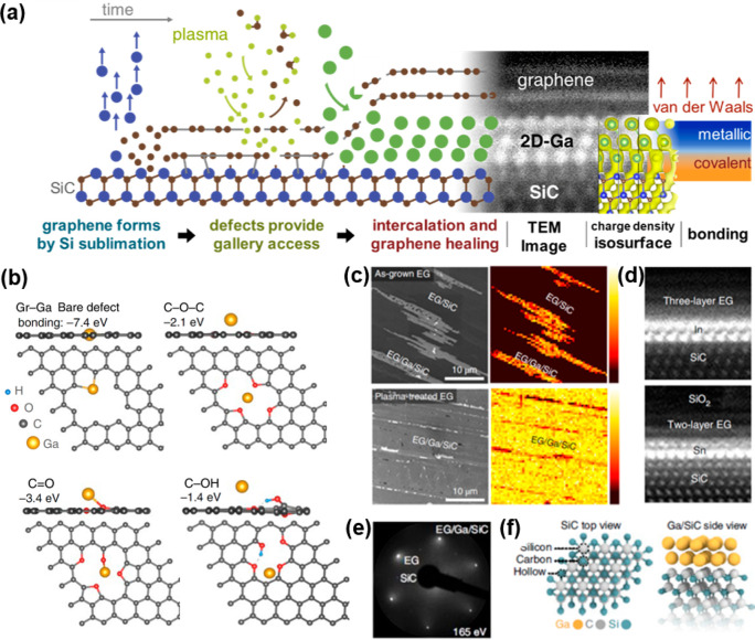
    1. Briggs N.; Bersch B.; Wang Y.; Jiang J.; Koch R. J.; Nayir N.; Wang K.; Kolmer M.; Ko W.; De La Fuente Duran A.; Subramanian S.; Dong C.; Shallenberger J.; Fu M.; Zou Q.; Chuang Y.-W.; Gai Z.; Li A.-P.; Bostwick A.; Jozwiak C.; Chang C.-Z.; Rotenberg E.; Zhu J.; van Duin A. C. T.; Crespi V.; Robinson J. A. Atomically thin half-van der Waals metals enabled by confinement heteroepitaxy. Nat. Mater. 2020, 19 (6), 637–643. 10.1038/s41563-020-0631-x. - DOI - PubMed
    1. Chhowalla M.; Shin H. S.; Eda G.; Li L. J.; Loh K. P.; Zhang H. The chemistry of two-dimensional layered transition metal dichalcogenide nanosheets. Nat. Chem. 2013, 5 (4), 263–75. 10.1038/nchem.1589. - DOI - PubMed