

Surface Smoothing by Atomic Layer Deposition and Etching for the Fabrication of Nanodevices
- PMID: 36583128
- PMCID: PMC9791650
- DOI: 10.1021/acsanm.2c04025
Surface Smoothing by Atomic Layer Deposition and Etching for the Fabrication of Nanodevices
Abstract
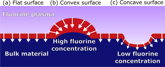
In many nano(opto)electronic devices, the roughness at surfaces and interfaces is of increasing importance, with roughness often contributing toward losses and defects, which can lead to device failure. Consequently, approaches that either limit roughness or smoothen surfaces are required to minimize surface roughness during fabrication. The atomic-scale processing techniques atomic layer deposition (ALD) and atomic layer etching (ALE) have experimentally been shown to smoothen surfaces, with the added benefit of offering uniform and conformal processing and precise thickness control. However, the mechanisms which drive smoothing during ALD and ALE have not been investigated in detail. In this work, smoothing of surfaces by ALD and ALE is studied using finite difference simulations that describe deposition/etching as a front propagating uniformly and perpendicular to the surface at every point. This uniform front propagation model was validated by performing ALD of amorphous Al2O3 using the TMA/O2 plasma. ALE from the TMA/SF6 plasma was also studied and resulted in faster smoothing than predicted by purely considering uniform front propagation. Correspondingly, it was found that for such an ALE process, a second mechanism contributes to the smoothing, hypothesized to be related to curvature-dependent surface fluorination. Individually, the atomic-scale processing techniques enable smoothing; however, ALD and ALE will need to be combined to achieve thin and smooth films, as is demonstrated and discussed in this work for multiple applications.
© 2022 The Authors. Published by American Chemical Society.
Conflict of interest statement
The authors declare no competing financial interest.
Figures


Similar articles
-
Advanced Fabrication of Ultrathin Ruthenium Films Using Synergistic Atomic Layer Deposition and Etching.Small Methods. 2025 Aug;9(8):e2402166. doi: 10.1002/smtd.202402166. Epub 2025 Mar 21. Small Methods. 2025. PMID: 40116341
-
Mechanisms of Thermal Atomic Layer Etching.Acc Chem Res. 2020 Jun 16;53(6):1151-1160. doi: 10.1021/acs.accounts.0c00084. Epub 2020 Jun 1. Acc Chem Res. 2020. PMID: 32476413
-
Competition between Al2O3 atomic layer etching and AlF3 atomic layer deposition using sequential exposures of trimethylaluminum and hydrogen fluoride.J Chem Phys. 2017 Feb 7;146(5):052819. doi: 10.1063/1.4973310. J Chem Phys. 2017. PMID: 28178819
-
Plasma-Assisted Nanofabrication: The Potential and Challenges in Atomic Layer Deposition and Etching.Nanomaterials (Basel). 2022 Oct 6;12(19):3497. doi: 10.3390/nano12193497. Nanomaterials (Basel). 2022. PMID: 36234624 Free PMC article. Review.
-
Advances in core technologies for semiconductor manufacturing: applications and challenges of atomic layer etching, neutral beam etching and atomic layer deposition.Nanoscale Adv. 2025 Apr 11;7(10):2796-2817. doi: 10.1039/d4na00784k. eCollection 2025 May 13. Nanoscale Adv. 2025. PMID: 40226206 Free PMC article. Review.
Cited by
-
Investigation of the atomic layer etching mechanism for Al2O3 using hexafluoroacetylacetone and H2 plasma.J Mater Chem C Mater. 2024 Nov 22;13(3):1345-1358. doi: 10.1039/d4tc03615h. eCollection 2025 Jan 16. J Mater Chem C Mater. 2024. PMID: 39583983 Free PMC article.
-
Recent advances in CMOS-compatible synthesis and integration of 2D materials.Nano Converg. 2025 Feb 15;12(1):11. doi: 10.1186/s40580-025-00478-1. Nano Converg. 2025. PMID: 39954210 Free PMC article. Review.
-
Development of an innovative low-temperature PEALD process for stress-compensated TiO2 and SiO2 multilayer anti-reflective coatings.Discov Nano. 2025 Mar 24;20(1):53. doi: 10.1186/s11671-025-04238-2. Discov Nano. 2025. PMID: 40128437 Free PMC article.
References
-
- Wang X.; Brown A. R.; Cheng B.; Asenov A.. Statistical Variability and Reliability in Nanoscale FinFETs. In Technical Digest - International Electron Devices Meeting, IEDM, 2011; pp 103–106.
-
- Lau W. S.; Yu D. Q.; Wang X.; Wong H.; Xu Y.. Confirmation of the Surface Smoothing Effect of Atomic Layer Deposition and the Physical Mechanism Responsible for Such an Effect. In China Semiconductor Technology International Conference 2016, CSTIC 2016, 2016; pp 3–5.
-
- Zhao Y.-P.; Wang G.-C.; Lu T.-M.; Palasantzas G.; de Hosson J. T. M. Surface-Roughness Effect on Capacitance and Leakage Current of an Insulating Film. Phys. Rev. B 1999, 60, 9157–9164. 10.1103/PhysRevB.60.9157. - DOI
-
- Yeh M. S.; Luo G. L.; Hou F. J.; Sung P. J.; Wang C. J.; Su C. J.; Wu C. T.; Huang Y. C.; Hong T. C.; Chen B. Y.; Chen K. M.; Wu Y. C.; Izawa M.; Miura M.; Morimoto M.; Ishimura H.; Lee Y. J.; Wu W. F.; Yeh W. K. Ge FinFET CMOS Inverters with Improved Channel Surface Roughness by Using In-Situ ALD Digital O3 Treatment. IEEE J. Electron Devices Soc. 2018, 6, 1232–1237. 10.1109/JEDS.2018.2878929. - DOI
-
- Tienda-Luna I. M.; Ruiz F. G.; Godoy A.; Biel B.; Gámiz F. Surface Roughness Scattering Model for Arbitrarily Oriented Silicon Nanowires. J. Appl. Phys. 2011, 110, 08451410.1063/1.3656026. - DOI
LinkOut - more resources
Full Text Sources