. 2023 Jan 1;12(1):3.
doi: 10.1038/s41377-022-01015-z.

Dielectric Mie voids: confining light in air

Affiliations

Dielectric Mie voids: confining light in air

Mario Hentschel et al. Light Sci Appl. .

Abstract

Manipulating light on the nanoscale has become a central challenge in metadevices, resonant surfaces, nanoscale optical sensors, and many more, and it is largely based on resonant light confinement in dispersive and lossy metals and dielectrics. Here, we experimentally implement a novel strategy for dielectric nanophotonics: Resonant subwavelength localized confinement of light in air. We demonstrate that voids created in high-index dielectric host materials support localized resonant modes with exceptional optical properties. Due to the confinement in air, the modes do not suffer from the loss and dispersion of the dielectric host medium. We experimentally realize these resonant Mie voids by focused ion beam milling into bulk silicon wafers and experimentally demonstrate resonant light confinement down to the UV spectral range at 265 nm (4.68 eV). Furthermore, we utilize the bright, intense, and naturalistic colours for nanoscale colour printing. Mie voids will thus push the operation of functional high-index metasurfaces into the blue and UV spectral range. The combination of resonant dielectric Mie voids with dielectric nanoparticles will more than double the parameter space for the future design of metasurfaces and other micro- and nanoscale optical elements. In particular, this extension will enable novel antenna and structure designs which benefit from the full access to the modal field inside the void as well as the nearly free choice of the high-index material for novel sensing and active manipulation strategies.


Conflict of interest statement

The authors declare no competing interests.

Figures
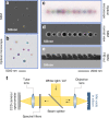
Fig. 1
Fig. 1. Resonant dielectric Mie voids.
Focused ion beam milling allows to structure conically shaped voids of varying diameter and depth into a bulk silicon wafer. a The scanning electron microscopy (SEM) image shows a random arrangement of holes of varying diameter and depth. b In the optical microscope image one can observe the wavelength-dependent resonant scattering from the individual voids. Evidently, diameter and depth contribute to the resonant behaviour. The same behaviour is observed for the chain of voids with 900 nm distance with varying size and depth. c Optical microscope image. d Top view SEM image, e Tilted SEM image of a focused ion beam cut. The distinct colour impression of each void can clearly be resolved in the optical microscope image. These experiments underpin the resonant and localized nature of the observed modes, which depend both on depth and diameter (or volume). f Sketch of the experimental setups used. The surface of the silicon is illuminated with white light and the reflected light is collected. The setups allow to control the angle of incidence via apertures. Additionally, spectral filters (band pass filters) allow to image the structures at specific wavelength down into the UV spectral range
Fig. 2
Fig. 2. Mie’s theory for silicon particles in air and air voids in Si.
a Field profiles and dispersion relations for localized Mie modes of a solid silicon Mie sphere in air and b, of a Mie void, which is, a spherical void inside an isotropic silicon environment. In both cases, Mie theory predicts the existence of localized modes (electric and magnetic dipole as well as quadrupole and higher-order modes). In spite of the inversed geometry, the modes show strong resemblance, yet, differ in the degree of confinement to the silicon and air, respectively. The dispersion relation of the modes of the silicon sphere is strongly influenced by the spectral dependence of the silicon refractive index and absorption (see c). For the Mie voids, in contrast, we observe perfectly linear dispersion, showing that the modes are fully localized in air without any noticeable influence of the silicon dispersion. c Real part n and imaginary part κ of the refractive index of silicon (upper panel) in comparison to the properties of the sphere and void modes (middle and lower panel, respectively). The graphs show the quality factors of each of the four fundamental modes for the sphere and void vs. the resonant wavelength of each of these modes. The dependence of the quality factor on the resonant wavelength is calculated by sweeping the sphere and void size. In case of the sphere (middle panel), one observes a drastic reduction of the quality factor for resonant wavelength approaching 400 nm and no modes are observed for wavelengths < 380 nm. This behaviour can be explained by the material losses in silicon, depicted with a dashed line showing the material quality factor n/2k. In case of the void (lower panel) the modes are confined within the air void. Consequently, the losses in silicon do not lead to a damping of the modes but rather result in a stronger confinement of the mode in the void by virtue of increased Fresnel reflection coefficient at the air-silicon interface (increased refractive index and increased absorption). Consequently, one can excite strongly confined modes in the deep-blue and UV spectral ranges with quality factors up to 35
Fig. 3
Fig. 3. Observation of Mie void modes.
a SEM images of holes with a diameter of 610 nm and a depth of 410 nm arranged in a square grid of 900 nm periodicity in order to allow for spectroscopic measurement. The tilted view image of the same structures shows slightly inclined side walls, which are intrinsic to the milling process. The lowest image depicts a focused ion beam cut of holes with a 780 nm diameter viewed at a tilting angle of 80° underpinning the conical shape. b Experimental and simulated normal incidence reflectance spectra of Mie voids in the silicon substrate. With increasing diameter, the fundamental mode I red-shifts while a higher-order mode II emerges, undergoing a spectral red-shift with increase of the diameter as well. c Spatial distribution of the absolute value of the internal electric field for light incident along the Z-axis and polarized along the X-axis for the second largest Mie void. The observed field distributions at points I and II can be identified as the two fundamental modes predicted by Mie’s theory in Fig. 2, which are electric and magnetic-dipole modes, respectively (for details see Supplementary Fig. S8)
Fig. 4
Fig. 4. Experimental observation of modes in the UV and visible spectral range.
a White light reflection image of an array of dielectric voids in silicon. The size as well as the depth are varied in 36 steps each. The diameters range from ~330 nm to 750 nm and the depth from ~20 nm to 1100 nm (all parameters can be found in the Supporting Information). b SEM images taken from the void array at the positions indicated in (a). The images are taken for the smallest diameter voids for smallest and highest dose (shallowest (iii) and deepest voids (i), respectively) as well as for the largest void diameter for smallest and highest dose (shallowest (iv) and deepest (ii) voids, respectively). c Experimental and simulated monochromatic images of the void array for the indicated wavelengths (displayed as vertical labels on the left). In the experiments, band pass filters at the specified centre wavelength are used to limit the wavelength range. With decreasing wavelength, an increasing number of modes can be observed. Due to the shorter wavelength, more and more higher-order modes can be resonantly excited. It is noteworthy, that this behaviour depends both on the depth as well as the diameter, ruling out trivial interference effects. In the UV spectral range at 265 nm or 4.7 eV, one experimentally observes seven distinct higher-order modes. The simulated optical response is in good agreement with the experiment
Fig. 5
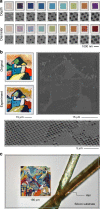
Fig. 5. Colour printing using Mie voids in a silicon substrate at 36.000 dpi.
Due to the ideal quality factor and thus linewidth of the Mie void modes, the structures show brilliant and naturalistic colours in reflection. Aided by the large interaction cross section, one Mie void is sufficient for one pixel. This gives our printing method a pointillistic touch, being completely different from grating-based approaches. a Selected sizes and depth of Mie voids and their colour impression in an optical microscope. b Detail taken from the painting “Improvisation No. 9” by Wassily Kandinsky (Staatsgalerie Stuttgart). The top left depicts the original artwork while the lower left shows an optical microscope image of the colour-printed image. In the SEM image on the right, one can clearly identify the image as the pixel size is unchanged. In order to gain access to the full colour space, the diameter as well as the depth of the Mie voids has been varied, which is particularly well visible in the tilted SEM image. c Fully reproduced “Improvisation No. 9” in a silicon substrate. The image consists of 200 pixels x 200 pixels and has a side length of 180 µm, corresponding to 36.000 dpi resolution. The image is shown next to a human hair for size comparison

References

    1. Halas NJ, et al. Plasmons in strongly coupled metallic nanostructures. Chem. Rev. 2011;111:3913–3961. doi: 10.1021/cr200061k. - DOI - PubMed
    1. Yu NF, Capasso F. Flat optics with designer metasurfaces. Nat. Mater. 2014;13:139–150. doi: 10.1038/nmat3839. - DOI - PubMed
    1. Curto AG, et al. Unidirectional emission of a quantum dot coupled to a nanoantenna. Science. 2010;329:930–933. doi: 10.1126/science.1191922. - DOI - PubMed
    1. Novotny L, Hulst Van. N. Antennas for light. Nat. Photonics. 2011;5:83–90. doi: 10.1038/nphoton.2010.237. - DOI
    1. Kauranen M, Zayats AV. Nonlinear plasmonics. Nat. Photonics. 2012;6:737–748. doi: 10.1038/nphoton.2012.244. - DOI