. 2023 Jan 1;13(1):195.
doi: 10.3390/nano13010195.

Metal-Dielectric Nanopillar Antenna-Resonators for Efficient Collected Photon Rate from Silicon Carbide Color Centers

Affiliations

Metal-Dielectric Nanopillar Antenna-Resonators for Efficient Collected Photon Rate from Silicon Carbide Color Centers

Faraz Ahmed Inam et al. Nanomaterials (Basel). .

Abstract

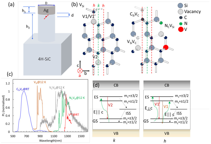
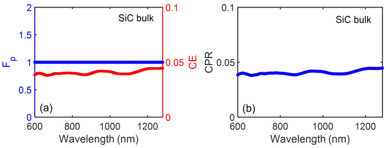
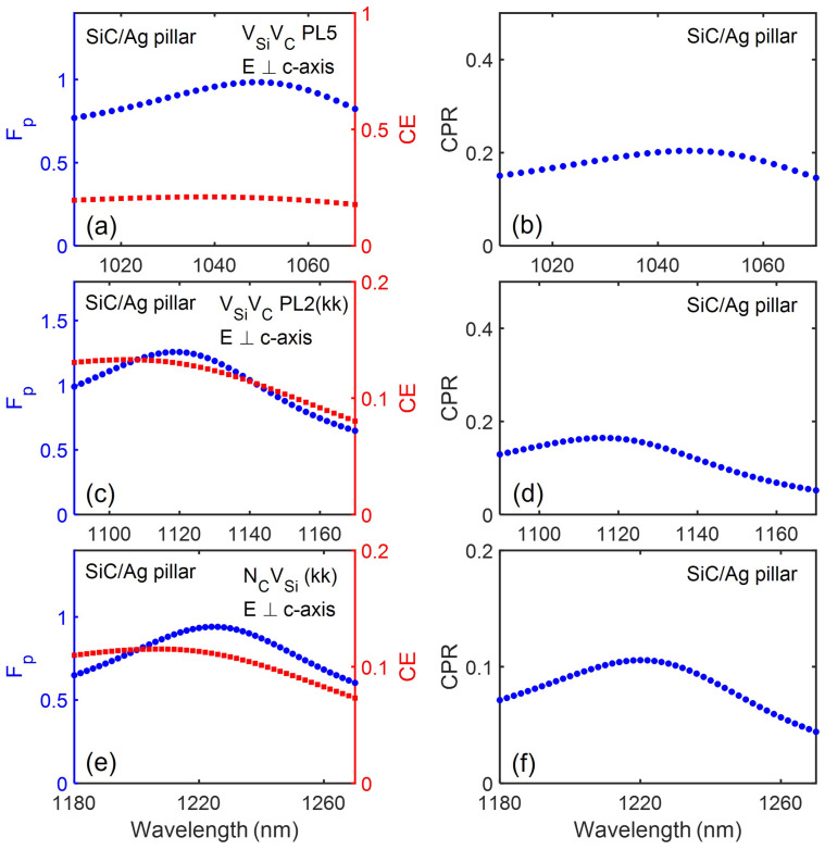
A yet unresolved challenge in developing quantum technologies based on color centres in high refractive index semiconductors is the efficient fluorescence enhancement of point defects in bulk materials. Optical resonators and antennas have been designed to provide directional emission, spontaneous emission rate enhancement and collection efficiency enhancement at the same time. While collection efficiency enhancement can be achieved by individual nanopillars or nanowires, fluorescent emission enhancement is achieved using nanoresonators or nanoantennas. In this work, we optimise the design of a metal-dielectric nanopillar-based antenna/resonator fabricated in a silicon carbide (SiC) substrate with integrated quantum emitters. Here we consider various color centres known in SiC such as silicon mono-vacancy and the carbon antisite vacancy pair, that show single photon emission and quantum sensing functionalities with optical electron spin read-out, respectively. We model the dipole emission fluorescence rate of these color centres into the metal-dielectric nanopillar hybrid antenna resonator using multi-polar electromagnetic scattering resonances and near-field plasmonic field enhancement and confinement. We calculate the fluorescence collected photon rate enhancement for these solid state vacancy-centers in SiC in these metal-dielectric nanopillar resonators, showing a trade-off effect between the collection efficiency and radiative Purcell factor enhancement. We obtained a collected photon rate enhancement from a silicon monovacancy vacancy center embedded in an optimised hybrid antenna-resonator two orders of magnitude larger compared to the case of the color centres in bulk material.

Keywords: Mie scattering; emission electromagnetic-dynamics; fluorescence collection enhancement; nanopillars; silicon carbide; single-photon sources; vacancy silicon.


Conflict of interest statement

The authors declare no conflict of interest.

Figures

Figure 1
Figure 1
(a) Nanopillar antenna-resonator in 4H-SiC and Ag, where optimization of the nanopillar and antenna height (h1,2), nanopillars diameter (D), dipole distance from the antenna (d) are studied. (b) Crystallographic representation of 4H-SiC with hexagonal (h) and cubic (k) sites location for Si and C, showing the h and k sites for the VSi and the h site for carbon vacancy pair (CSiVC) and NCVSi, and the k site for the divacancy VCVSi and Vanadium (V). The direction of the c-axis is also shown. (c) Spectroscopy at room and low temperature of here studied color centres. Single CSiVC at room temperature (RT) measured using a home-built scanning confocal microscope with 532 nm excitation as described in ref. [27] based on samples fabricated as described in ref. [28]. Ensemble of VSi implanted on a c-face grown 4H-SiC, showing the ZPLs of the V1/V1’ lines for the centre at the h site and the V2 line for the centres at the k site. As the substrate is grown on the c-face the dominant emission is the V1’ due to its dipole laying in the plane of the substrate (excited by a laser perpendicular to the c-axis). Additional PL at 12 K of ensemble of VSiVC, NSiVC and RT V+4. VSi, VSiVC, and NSiVC are excited using 780 nm and 976 nm respectively and measured using a commercial Horiba Raman system and home built confocal systems operating at low and room temperature equipped with infrared spectrometer and single photon detectors as described in ref. [12,27]. Samples are created as described in ref [12]. V+4 was not measured but deduced from ref. [29]. (d) Schematic of the energy levels (Ground state, GS, excited state, ES, and intersystem state, ISS) of the V1’/V1 and V2 emitters, showing that V1 and V2 are excited with an electric field parallel to the c-axis, while V1’ with an electric field perpendicular to the c-axis.
Figure 2
Figure 2
(a) The modified Purcell factor, Fp and collection efficiency, CE and (b) the corresponding CPR performance for a point dipole emitter in bulk SiC as a function of the emission wavelength.
Figure 3
Figure 3
The modified Purcell factor, Fp, (a,c,e) and collection efficiency, CE; the corresponding CPR performance for various point defect emitters in SiC pillar (b,d,f). The specified color centres dipole is located 20 nm below the Ag cylinder surface with the given polarisations.
Figure 4
Figure 4
The modified Purcell factor, Fp and collection efficiency, CE (a,c,e); the corresponding CPR performance for various point defect emitters in SiC pillar (b,d,f). The specified color centres dipole is located 20 nm below the Ag cylinder surface with the given polarisation.
Figure 5
Figure 5
(a) The modified Purcell factor, Fp and collection efficiency, CE; (b) the corresponding CPR performance as a function of the SiC pillar’s height variation for an embedded point defect emitters in SiC pillar emitting at 917 nm. The specified color centres dipole is located 20 nm below the Ag cylinder surface with polarisation along the c-axis.
Figure 6
Figure 6
The 2-D normalised electric field pattern for a point dipole emission in (a) bulk SiC and (b) coupled SiC pillar/Ag antenna scheme optimized at 917 nm.
Figure 7
Figure 7
Far-field 2-D radiation patterns for a point dipole emission in (a) bulk SiC at 917 nm and SiC pillar at (b) 917 nm and (c) 649 nm, respectively.

References

    1. Awschalom D.D., Hanson R., Wrachtrup J., Zhou B.B. Quantum technologies with optically interfaced solid-state spins. Nat. Photonics. 2018;12:516–527. doi: 10.1038/s41566-018-0232-2. - DOI
    1. Atatüre M., Englund D., Vamivakas N., Lee S.Y., Wrachtrup J. Material platforms for spin-based photonic quantum technologies. Nat. Rev. Mater. 2018;3:38–51. doi: 10.1038/s41578-018-0008-9. - DOI
    1. Castelletto S., Boretti A. Silicon carbide color centers for quantum applications. J. Phys. Photonics. 2020;2:022001. doi: 10.1088/2515-7647/ab77a2. - DOI
    1. Ahmed N., Akhtar S., Inam F.A. Hyperbolic metamaterial-based metal–dielectric resonator-antenna designs for GHz photon collection rates from wide-range solid-state single-photon sources. J. Opt. Soc. Am. B. 2020;37:3469. doi: 10.1364/JOSAB.402890. - DOI
    1. Karamlou A., Trusheim M.E., Englund D. Metal-dielectric antennas for efficient photon collection from diamond color centers. Opt. Express. 2018;26:3341–3352. doi: 10.1364/OE.26.003341. - DOI - PubMed

LinkOut - more resources