Review
. 2023;3(1):1.
doi: 10.1186/s43593-022-00027-x. Epub 2023 Jan 4.

Prospects and applications of on-chip lasers

Affiliations
Review

Prospects and applications of on-chip lasers

Zhican Zhou et al. eLight. 2023.

Abstract

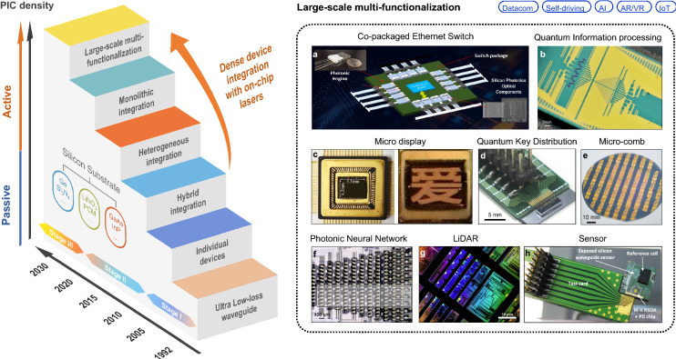
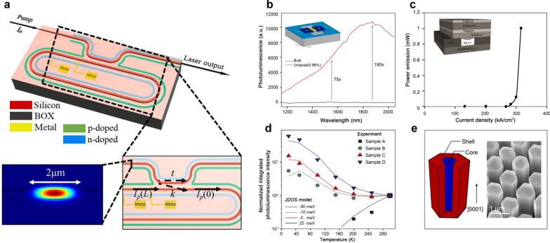
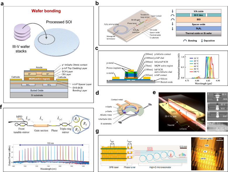
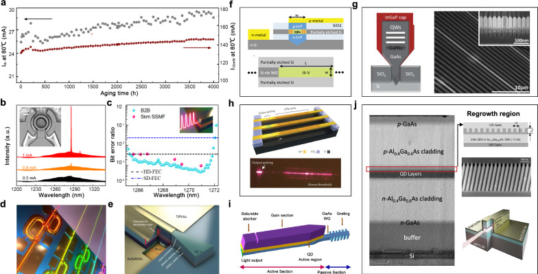
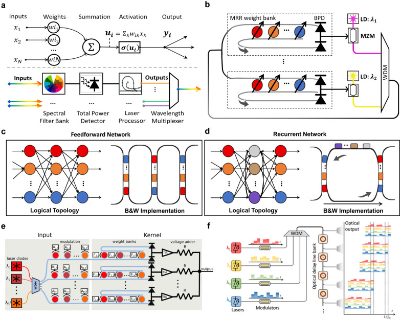
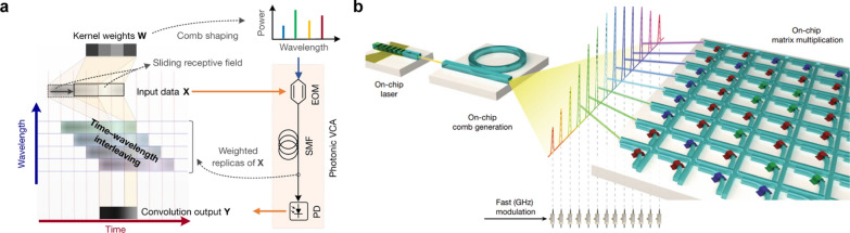
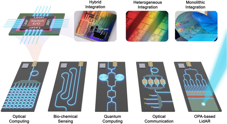
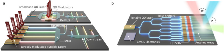
Integrated silicon photonics has sparked a significant ramp-up of investment in both academia and industry as a scalable, power-efficient, and eco-friendly solution. At the heart of this platform is the light source, which in itself, has been the focus of research and development extensively. This paper sheds light and conveys our perspective on the current state-of-the-art in different aspects of application-driven on-chip silicon lasers. We tackle this from two perspectives: device-level and system-wide points of view. In the former, the different routes taken in integrating on-chip lasers are explored from different material systems to the chosen integration methodologies. Then, the discussion focus is shifted towards system-wide applications that show great prospects in incorporating photonic integrated circuits (PIC) with on-chip lasers and active devices, namely, optical communications and interconnects, optical phased array-based LiDAR, sensors for chemical and biological analysis, integrated quantum technologies, and finally, optical computing. By leveraging the myriad inherent attractive features of integrated silicon photonics, this paper aims to inspire further development in incorporating PICs with on-chip lasers in, but not limited to, these applications for substantial performance gains, green solutions, and mass production.

Keywords: Communication; LiDAR; On-chip lasers; Optical computing; Photonic integration; Silicon photonics.


Conflict of interest statement

Competing interestsThe authors declare no conflict of interest.

Figures

Fig. 1
Fig. 1
Progress of silicon-based photonic integration with different development stages since 1992. Examples of Large-scale multi-functionalization are listed: a Co-packaged Ethernet Switch. Image credit: Intel [17]. b Quantum Information processing. Adapted with permission from [18], copyright 2022, AAAS. c Micro display. Adapted with permission from [19], copyright 2021, IEEE. d Quantum Key Distribution (QKD). Adapted with permission from [20], copyright 2019, NPG. e Micro-comb. Adapted with permission from [21], copyright 2021, AAAS. f Photonic Neural Network Adapted with permission from [22], copyright 2017, NPG. g LiDAR Image credit: MIT Lincoln Laboratory [23]. h Sensor. Adapted with permission from [24], copyright 2019, SPIE
Fig. 2
Fig. 2
Concepts for on-chip silicon-based lasers using group-IV materials. a Silicon Raman racetrack ring laser Adapted with permission from [31], copyright 2022, WILEY. b Micromachining-based GOI structure realizes direct-bandgap light-emitting under tensile strain. Adapted with permission from [37], copyright 2012, NPG. c The first electrically pumped Ge laser at room temperature (combination of tensile strain and n-type doping). Adapted with permission from [38], copyright 2012, OPG. d Lasing in a direct-bandgap group IV system created by alloying GeSn without mechanically introducing strain. Adapted with permission from [40], copyright 2012, AIP. e Light emission from direct-bandgap hexagonal Ge and SiGe alloys. Adapted with permission from [26], copyright 2020, NPG
Fig. 3
Fig. 3
Heterogeneous integration technology. a A schematic illustration of the bonding process. b A fully integrated Si3N4-based laser through multiple wafer bonding. Adapted with permission from [58], copyright 2020, OPG. c A heterogeneously-integrated QCL with the longest wavelength at 4.8 μm. Adapted with permission from [63], copyright 2016, OPG. d Compact low-threshold micro-ring lasers with heterogeneously integrated QD epitaxial material as an active layer. Adapted with permission from [65], copyright 2019, OPG. e Heterogeneously integrated QD-DFB lasers with efficient light coupling to the silicon waveguide. Adapted with permission from [66], copyright 2021, WILEY. f Widely tunable lasers using a coupled-triple ring structure. Adapted with permission from [69], copyright 2019, IEEE. g Laser soliton microcombs. Adapted with permission from [21], copyright 2021, AAAS
Fig. 4
Fig. 4
Monolithic integration. a Robust laser operation at 80 °C with >1 M hour extrapolated lifetime. Adapted with permission from [84], copyright 2021, OPG. Individual QD lasers directly grown on silicon with b submilliamp threshold microring lasers, c mode-locked lasers, d coupled cavity tunable lasers and e DFB lasers. Adapted with permission from [–88], copyright 2017 & 2019, OPG. f Schematic illustration of a selectively grown III–V cavity onto the handle wafer of an SOI substrate. Selective growth of box-shaped III-V materials on silicon for g a GaAs based nano-ridge laser array and h InP based DFB laser array. Adapted with permission from [–91], copyright 2015 & 2017, OPG & NPG. i A monolithic offset QD integration platform where the light from QD active region is coupled to passive GaAs waveguides. Adapted with permission from [93], copyright 2020, OPG. j A regrown III-V QD-DFB laser that can combine different bandgaps into one optical chip. Adapted with permission from [94], copyright 2020, WILEY
Fig. 5
Fig. 5
Development of silicon photonics-based LiDAR. The first silicon photonics-based OPA. Adapted with permission from [108], copyright 2009, OPG. A large-scale two-dimensional OPA with complex far-field patterns. Adapted with permission from [109], copyright 2013, NPG. III-V/ silicon beam scanner with lasers. Adapted with permission from [111], copyright 2015, OPG. Monolithic 2D OPA with independent integrated electric control. Adapted with permission from [112], copyright 2015, OPG. High-resolution OPA based on non-uniform waveguide arrays. Adapted with permission from [113], copyright 2016, OPG. Extremely low static power consumption OPA system based on III-V/silicon phase shifter arrays. Adapted with permission from [114], copyright 2019, OPG. The first packaged coherent OPA-based LiDAR on a silicon photonic platform. Adapted with permission from [115], copyright 2019, IEEE. Mobile Eye’s integrated FMCW LiDAR. Image credit: Intel [116]. The first large-scale OPA-based silicon photonic LiDAR with on-chip array calibration capability. Adapted with permission from [117], copyright 2021, IEEE
Fig. 6
Fig. 6
Silicon photonic sensors for chemical and biological analysis. Spectroscopic sensing, a The fully integrated packaged silicon photonic CH4 sensor. Adapted with permission from [129], copyright 2017, OPG. b The Chip-scale Sarin gas silicon photonics sensor. Adapted with permission from [126], copyright 2019, SPIE. c Wearable silicon photonics biomarker monitor based on Raman spectroscopy. Image credit: Rockley [130]. Refractive-index-based sensing. d Genalyte’s biosensor based on microring arrays. Adapted with permission from [131], copyright 2015, ACS. e A nanophotonic biosensor based on the BiMW interferometer. Adapted with permission from [132], copyright 2021, IOP. f An integrated photonic biosensor prototype for cancer diagnosis Image credit: PHIX [133]
Fig. 7
Fig. 7
Key milestones in silicon-based IQP. On-chip quantum interference and integrated CNOT gate on SiO2. Adapted with permission from [138], copyright 2008, AAAS. Integrated silicon SNSPD. Adapted with permission from [139], copyright 2012, NPG. The first integration of single-photon sources with quantum circuits on silicon. Adapted with permission from [140], copyright 2014, NPG. Chip-to-chip entanglement distribution system between two silicon chips. Adapted with permission from [141], copyright 2016, OPG. On-chip generation of six photons. Adapted with permission from [142], copyright 2017, OPG. The fully programmable two-qubit quantum processor on silicon [143], large-scale silicon IQP device comprising over 670 optical components. Adapted with permission from [18], copyright 2018, AAAS. The tunable AlGaAs-on-insulator (AlGaAsOI) MRR entangled-photon-pair source and all-on-chip quantum photonic circuits. Adapted with permission from [144], copyright 2021, APS. Topologically quantum entanglement emitter with a high tolerance of fabrication. Adapted with permission from [145], copyright 2022, NPG
Fig. 8
Fig. 8
Silicon-based integrated quantum photonic applications. a The first field tests for a metropolitan QKD connected by optical fiber.Adapted with permission from [152]. copyright 2018, APS. b Daylight free-space QKD using silicon photonic circuits. Adapted with permission from [153], copyright 2021, NPG. c A programmable qudit-based quantum processor in silicon-based IQP circuits. Adapted with permission from [154], copyright 2022, NPG. d A quantum photonic simulator and diamond nitrogen-vacancy center. Adapted with permission from [155] copyright 2017, NPG
Fig. 9
Fig. 9
Schematics of the B&W architecture for neural networks. a The B&W architecture (bottom) shows parallels with the neuron model (top). Adapted with permission from [164], copyright 2014, OPG. b Concept of a B&W network with MRR arrays as the spectral filters. Adapted with permission from [165], copyright 2017, NPG. cd Different mapping topologies for photonic neural networks, e.g., c feedforward network and d recurrent network. Adapted with permission from [174], copyright 2018, IEEE. e An optoelectrical architecture that performs a single convolution window. Adapted with permission from [175], copyright 2020, IEEE. f Conceptual layout of an optical patching scheme. Adapted with permission from [, copyright 2020, OPG
Fig. 10
Fig. 10
a Illustration of the photonic vector convolutional accelerator that interleaves temporal, wavelength and spatial dimensions. Adapted with permission from [178], copyright 2021, NPG. b A fully integrated photonic tensor core for parallel convolutional processing, taking advantage of the in-memory computing technology. Adapted with permission from [179], copyright 2021, NPG
Fig. 11
Fig. 11
PICs in different system-level applications with integrated on-chip lasers via different integration techniques. Insets adapted with permission from [21, 189, 190], copyright 2016 & 2021, OPG & AAAS & NPG
Fig. 12
Fig. 12
Integrated QD lasers for: a optical WDM communications and b OPA-based LiDAR applications

References

    1. "Cisco Annual Internet Report (2018–2023) White Paper," Cisco, Mar 9 2020. Accessed: Jun 21, 2022. [Online]. https://www.cisco.com/c/en/us/solutions/collateral/executive-perspective...
    1. Nagarajan R, et al. Large-scale photonic integrated circuits. IEEE J. Sel. Top. Quantum Electron. 2005;11:50–65. doi: 10.1109/JSTQE.2004.841721. - DOI
    1. Hou J, Situ G. Image encryption using spatial nonlinear optics. eLight. 2022;2:1–10. doi: 10.1186/s43593-021-00010-y. - DOI
    1. Li L, Zhao H, Liu C, Li L, Cui TJ. Intelligent metasurfaces: control, communication and computing. eLight. 2022;2:1–24. doi: 10.1186/s43593-022-00013-3. - DOI
    1. Miller DA. Device requirements for optical interconnects to silicon chips. Proc. IEEE. 2009;97:1166–1185. doi: 10.1109/JPROC.2009.2014298. - DOI