Review
. 2022 May 18;15(1):24.
doi: 10.1007/s12200-022-00017-4.

Optical metalenses: fundamentals, dispersion manipulation, and applications

Affiliations
Review

Optical metalenses: fundamentals, dispersion manipulation, and applications

Yongli He et al. Front Optoelectron. .

Abstract

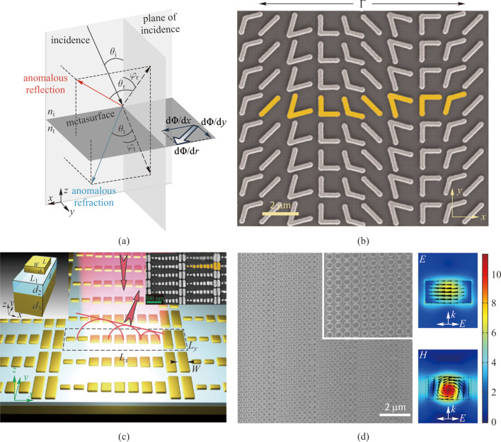
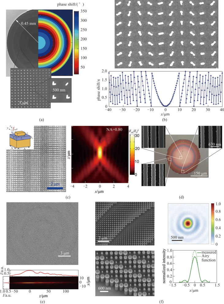
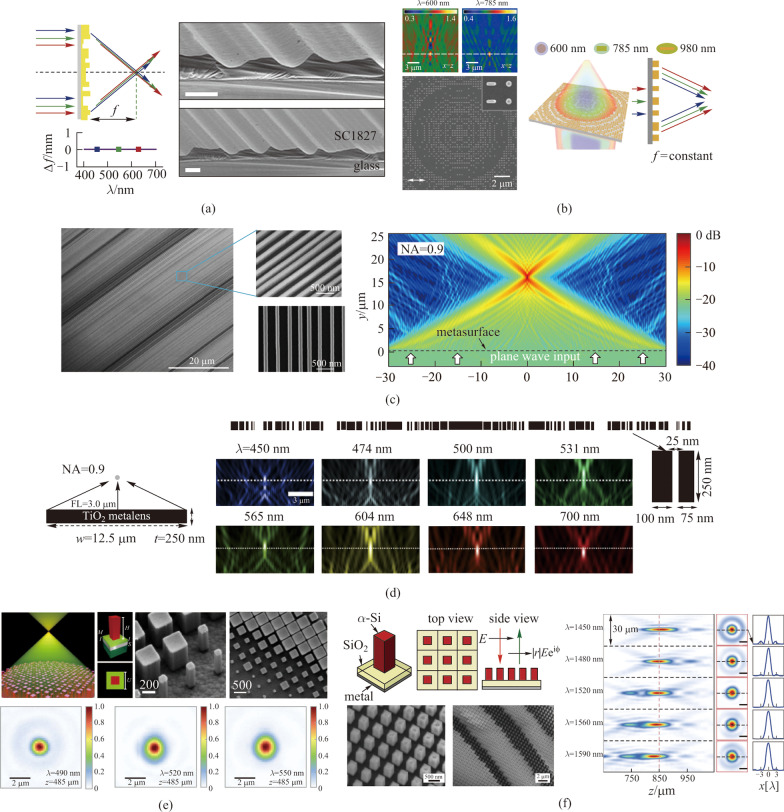
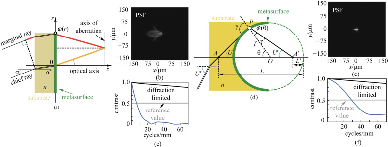
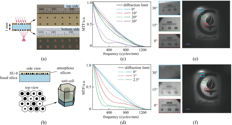
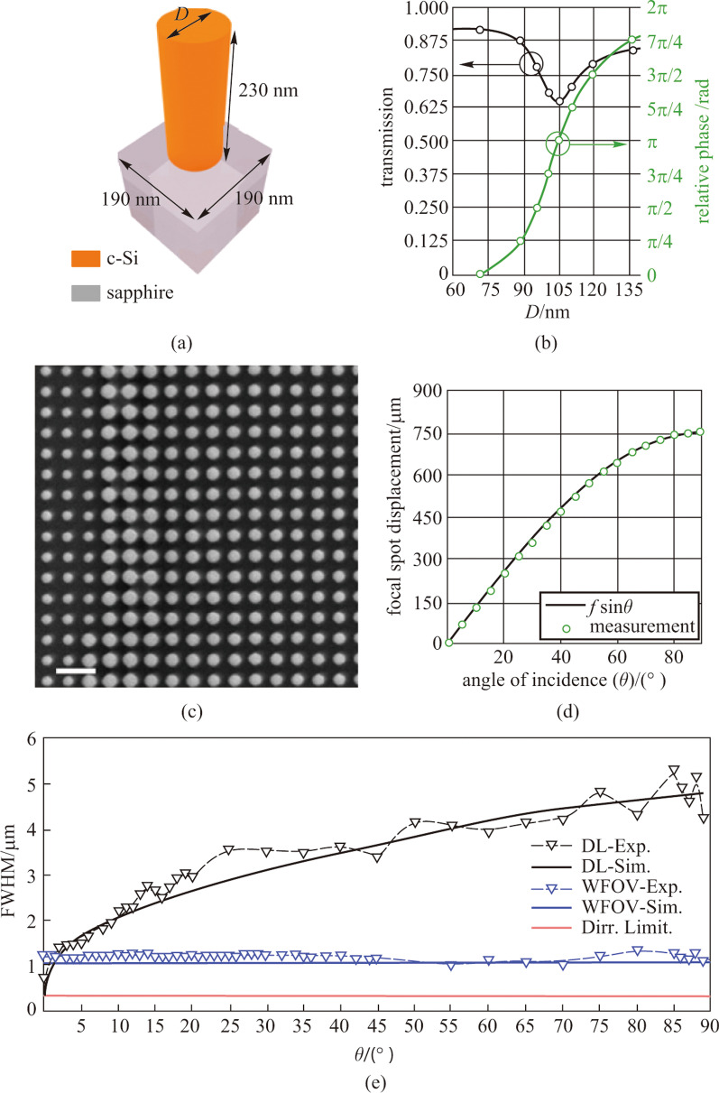
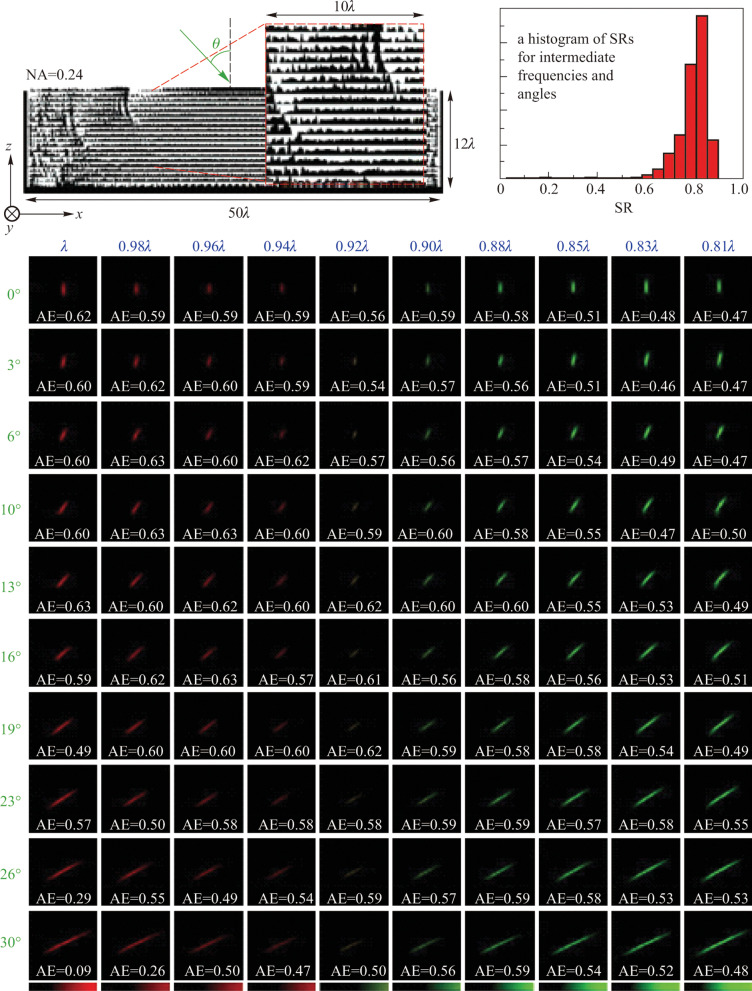
Metasurfaces, also known as 2D artificial metamaterials, are attracting great attention due to their unprecedented performances and functionalities that are hard to achieve by conventional diffractive or refractive elements. With their sub-wavelength optical scatterers, metasurfaces have been utilized to freely modify different characteristics of incident light such as amplitude, polarization, phase, and frequency. Compared to traditional bulky lenses, metasurface lenses possess the advantages of flatness, light weight, and compatibility with semiconductor manufacture technology. They have been widely applied to a range of scenarios including imaging, solar energy harvesting, optoelectronic detection, etc. In this review, we will first introduce the fundamental design principles for metalens, and then report recent theoretical and experimental progress with emphasis on methods to correct chromatic and monochromatic aberrations. Finally, typical applications of metalenses and corresponding design rules will be presented, followed by a brief outlook on the prospects and challenges of this field.

Keywords: Chromatic and monochromatic aberrations; Flat optics; Metalenses; Metasurfaces; Nanophotonics.


Conflict of interest statement

The authors declare that they have no competing interests.

Figures

Fig. 1
Fig. 1
Pioneer works demonstrating the fundamental design rules. a Schematics of the generalized Snell’s law of reflection and refraction. The gradient of phase shift dΦ/dr at the interface offers an effective wavevector that can bend reflected and transmitted light in designed directions. b Scanning electron microscope (SEM) image of the plasmonic metasurface with V-shaped optical antennas. c Schematic of the reflect-array metasurface with gold patch antennas separated from a gold substrate by a dielectric spacer with subwavelength thickness. The left inset shows a schematic of an individual unit-cell, and the right inset is the corresponding SEM image of the metasurface. d SEM image of a dielectric metasurface Huygens’ beam deflector and the corresponding simulated field distributions. a Reprinted with permission of IOP Publishing, from Ref. [23]; permission conveyed through Copyright Clearance Center, Inc. b Reprinted from Ref. [13]. Copyright 2011, The American Association for the Advancement of Science. c Reprinted with permission from Ref. [24]. Copyright 2012, American Chemical Society. d Reprinted with permission from Ref. [25]. Copyright 2015, WILEY‐VCH Verlag GmbH & Co. KGaA, Weinheim
Fig. 2
Fig. 2
Typical examples of 2π phase coverage realization in light-concentrating metasurfaces. a SEM image of the metasurface with V-shaped antennas and the corresponding phase shift profile. b SEM image and expected phase discontinuity of a plasmonic metasurface on an ITO-coated glass substrate with positive polarity for incident lights with right circular polarization. c SEM image and measured intensity distribution near the focus of a cylindrical metalens with 0.8 NA. The inset shows the schematic of an individual unit cell. d Optical micrograph and SEM images of a high-contrast grating metalens. e SEM image of a geometric phase metasurface with dielectric microbars and corresponding measured intensity distribution along the propagation direction. f Top-view and side-view SEM images of the polarization insensitive metasurfaces, and the measured focal profile and corresponding horizontal cut of the focal spot at 532 nm. a Reprinted with permission from Ref. [12]. Copyright 2012, American Chemical Society. b Reprinted with permission from Ref. [34]. Copyright 2012, Chen et al. c Reprinted with permission from Ref. [35]. Copyright 2013, American Chemical Society. d Reprinted with permission from Ref. [36]. Copyright 2010, Springer Nature. e Reprinted with permission from Ref. [37]. Copyright 2014, The American Association for the Advancement of Science. f Reprinted with permission from Ref. [38]. Copyright 2016, American Chemical Society
Fig. 3
Fig. 3
Multiwavelength achromatic metalens. a Tandem-stacked multilayered plasmonic multiwavelength metalens designed using frequency-dependent scatterers. b Multiwavelength metalens multiplexed by segmentation. c Multiwavelength polarization-insensitive metalenses with unit cells composed of meta-atoms. d Metasurfaces consisting of coupled rectangular dielectric resonators as unit-cells to introduce the desired phase profiles simultaneously at three wavelengths (1300, 1550, and 1800 nm) with dispersion compensation. e Birefringent metalenses with elliptical meta-atoms designed to focus light with two different wavelengths and orthogonal polarizations. a Reprinted from permission from Ref. [47]. Copyright 2017, Avayu et al. b Reprinted with permission from Ref. [48], IOP Publishing, permission conveyed through Copyright Clearance Center, Inc. c Reprinted with permission from Ref. [52]. Copyright 2016, The Optical Society. d Reprinted with permission from Ref. [49]. Copyright 2015, American Chemical Society. e Reprinted with permission from Ref. [54]. Copyright 2016, The Optical Society
Fig. 4
Fig. 4
Broadband metalenses designed with different optimization algorithms. a Achromatic focusing at three discrete wavelengths (460, 540, and 620 nm) by chromatic-corrected diffractive metalenses optimized with direct-binary-search algorithm. b Multiwavelength achromatic lenses designed with lattice evolution algorithm. c Metalens with operation wavelengths from 580 to 700 nm range using topology optimization. d Achromatic metalenses with large NA via inverse design approach utilizing plane-wave mode decomposition. e An achromatic metalens over a continuous visible wavelength range made of TiO2 nanopillars, a dielectric spacer, and a metallic back reflector. f Dispersion-engineered metasurfaces over the wavelength range of 1450 to 1590 nm with minimized chromatic dispersion. a Reprinted with permission from Ref. [63]. Copyright 2016, Wang et al. b Reprinted with permission from Ref. [64]. Copyright 2016, American Chemical Society. c Reprinted with permission from Ref. [65]. Copyright 2019, Phan et al. d Reprinted with permission from Ref. [66]. Copyright 2020, The Optical Society. e Reprinted with permission from Ref. [67]. Copyright 2017, American Chemical Society. f Reprinted with permission from Ref. [68]. Copyright 2017, The Optical Society
Fig. 5
Fig. 5
Dispersion manipulation based on compensation phase. a Reflective broadband achromatic metalenses in the infrared range of 1200 to 1680 nm realized by Au integrated-resonant unit elements and new design principles. b Visible range achromatic metalenses operating from 400 to 667 nm achieved by Al integrated-resonant unit elements. c Transmissive achromatic metalens operating from 400 to 600 nm made of GaN nanopillars and nanoholes. d A full-color light field camera composed of multiple achromatic GaN metalens arrays. e A transmissive broadband achromatic metalens operating in the visible from 470 to 670 nm made of coupled TiO2 nanofins for each unit cell. a Reproduced with permission from Ref. [69]. Copyright 2017, Wang et al. b Reproduced with permission from Ref. [73]. Copyright 2018, WILEY‐VCH Verlag GmbH & Co. KGaA, Weinheim. c Reprinted with permission from Ref. [70]. Copyright 2018, Springer Nature Customer Service Centre GmbH: Springer Nature, Nature Nanotechnology. d Reprinted with permission from Ref. [71]. Copyright 2019, Springer Nature Customer Service Centre GmbH: Springer Nature, Nature Nanotechnology. e Reprinted with permission from Ref. [72]. Copyright 2018, Springer Nature Customer Service Centre GmbH: Springer Nature, Nature Nanotechnology
Fig. 6
Fig. 6
Polarization insensitive broadband metalens with isotropic symmetry. a Broadband achromatic metalenses made of libraries of meta-units with complex cross-sectional geometries to provide diverse phase dispersions for arbitrary polarization state from 1200 to 1650 nm. b A silicon nitride metalens in the visible region with zero effective material dispersion and an effective achromatic refractive index distribution from 430 to 780 nm. a Reprinted with permission from Ref. [74]. Copyright 2018, Shrestha et al. b Reprinted with permission from Ref. [75]. Copyright 2019, Fan et al.
Fig. 7
Fig. 7
Polarization insensitive broadband metalens with anisotropic unit-cells. a A broadband achromatic metalens with a NA of 0.2 over the visible range from 460 to 700 nm while simultaneously maintaining polarization-insensitive and diffraction-limited performances. b A metacorrector with a tunable phase and artificial dispersion to correct spherical and chromatic aberrations in a large spherical plano-convex lens. a Reprinted with permission from Ref. [76]. Copyright 2019, Chen et al. b Reprinted with permission from Ref. [77]. Copyright 2018, American Chemical Society
Fig. 8
Fig. 8
Novel meta-devices to control angular dispersion. a SEM images of the angular independent meta-absorber with symmetric and asymmetrical configurations. Px, Py are the periodicity along x and y directions, respectively. b Schematics of multifunctional metadevice for polarization conversion. Linear incident light can be converted to right-handed (RCP) or left-handed circular polarization (LCP) depending on incident angles. a Reprinted with permission from Ref. [78]. Copyright 2020, Zhang et al. b Reprinted with permission from Ref. [79]. Copyright 2018, American Physical Society
Fig. 9
Fig. 9
Aplanatic metalens. a A flat metalens illuminated by parallel rays incident at angle α. The OPD equals the red segment plus the equivalent OP of phase discontinuity λ2πϕ(r), subtracting the yellow segment. b Point spread function (PSF) and c modulation transfer function (MTF) of flat metalens. d Schematics of an aplanatic metalens with metasurface pattern on a spherical substrate. e PSF and f MTF of aplanatic metalens. The sidelobe here is significantly reduced compared with b. And the spatial resolution at minimum contrast 0.5 is enhanced from 8 to 30 cycles/mm. af Reprinted with permission from Ref. [80]. Copyright 2013, The Optical Society
Fig. 10
Fig. 10
Cascaded metalenses in the near infrared. a Schematic of the aberration-free metalens doublet focusing off-axis light. b Illustration of the dielectric metasurface used to implement the metalens. The metasurface array is composed of amorphous silicon posts with variant diameters and SU-8 polymer on top in hexagonal arrangement. The MTF of c polynomials doublet and d hyperbolic singlet metalens. The focal length and aperture diameter of both lens is set as the same. Image taken by e the doublet and f the singlet. af Reprinted with permission from Ref. [81]. Copyright 2016, Arbabi et al.
Fig. 11
Fig. 11
Metalens doublet in the visible: schematic illustration, SEM image and phase profile of the metasurface doublet. a Metalens doublet is comprised of two metasurfaces integrated on both sides of a SiO2 substrate. be Geometrical parameters of the TiO2 nanofins; ce side and top views of the hexagonal unit cell with constant periodic length S, nanofin height H, nanofin length L, width W, and variant rotation angle α. f Top-side view SEM micrograph of the focusing metalens. g Side view SEM micrograph at the edge of the sample. h Phase plot of aperture metalens. i Comparison of phase plots of hyperbolic metalens and that of focusing metalens designed based on Eq. (10). jl Ray diagrams to depict the principle of aberration correction. j Ray diagram of hyperbolic metalens which shows large aberration at oblique illuminance. k Ray diagram of metalens with phase profile designed according to light blue curve in Fig. 9g, which shows positive and negative spherical aberration. l Ray diagrams of the metalens doublet showing diffraction-limited focusing at all angles. al Reprinted with permission from Ref. [82]. Copyright 2017, American Chemical Society
Fig. 12
Fig. 12
Wide-angle metalens with aperture stop. a Schematic of the hexagon unit cell composed of SiO2 nanopost placed on GaN substrate with fixed height 600 nm. b Simulated images of USAF-1951 test chart with traditional lens and c wide-angle metalens. d Traditional lens layout. e Traditional lens Strehl ratio. f Traditional lens MTF. g Metalens layout. h Metalens Strehl ratio. i Metalens MTF. The NA of the optical system in both the designs is set to 0.18, and the cutoff frequency is approximately 600 in cycle per mm. ai Reprinted with permission from Ref. [86]. Copyright 2020, Fan et al.
Fig.13
Fig.13
Proof-of-concept quadratic phase metalens. a Ray diagram of wide-angle flat lens illuminated by oblique rays. Red, yellow and blue rays are corresponding to different incident angles. The lens transforms the difference in incident angles into traverse shifts of focuses on the focal plane. b Ray diagram of an ordinary lens and a quadratic flat lens at normal illumination. Spherical aberration is introduced in the quadratic lens. c Top: SEM of the fabricated metalens with elliptical aperture arrays on a gold film. Bottom left: simulated results of light intensity distributions on xz (y = 0) and xy (z = 7.5 μm) plane at 632.8 nm with 0,-32,-80,and45 incident angles. Bottom right: experimental measurement of light intensity distribution on xz plane at θ=0,-32 and θ=0,-80. The FWHM is about 427 nm. d Top: schematic of measurement set up to demonstrate the multiwavelength behavior. Bottom: intensity distribution in a common focal plane shows clear spots for three wavelengths. ad Reprinted with permission from Ref. [93]. Copyright 2017, The Optical Society
Fig. 14
Fig. 14
Quadratic phase metalens with arbitrarily wide FOV. a Schematic of the c-Si nanopost unit cell with fixed period a = 190 nm and height h = 230 nm. b Transmission and phase map. D refers to the diameters of c-Si nanoposts and the cycle marks represent the eight phase levels used to discretize the phase profile. c SEM micrograph of the c-Si nanopost array (top view). d Measured displacement of the focal spot as a function of incident angels. e Measured and simulated FWHM versus incident angles curves of hyperbolic (referred to as D.L. in the graph) and quadratic (referred to as WFOV) lens. ae Reprinted with permission from Ref. [92]. Copyright 2020, American Chemical Society
Fig. 15
Fig. 15
Inverse designed single-piece multilayer metalens that simultaneously corrects chromatic and angular aberrations. Top-left is the schematic of the metalens consisting of 20 layers of 3D-printable polymers with NA = 0.24. Top-right inset shows the distribution of Strehl ratio (SR) of intermediate frequencies and angles within the designated bandwidth and FOV. Most SRs remain higher than 0.7 and the mean value is larger than 0.75. The bottom shows the cross-section light field distributions and AEs of the designed wavelengths and angles (N = 10 × 10 = 100). The average of AEs is as high as 55%. Reprinted with the permission from Ref. [61]. Copyright 2021, AIP Publishing
Fig. 16
Fig. 16
Spectral tomographic imaging system based on aplanatic metalens. a Calculated focusing efficiency of the unit cell over working wavelength. The inset is a schematic of the unit cell composed of GaN nanopost placed on sapphire. b Optical (left) and SEM (right) images of the fabricated metalens. c Schematic of the imaging setup. The inset shows four images obtained by an objective O2 acting as objects to verify the tomographic imaging of the metalens. Images captured by d aplanatic and e normal metalens through the objective O1 and CCD at different wavelengths are shown. f Microscopic tomography of frog egg cells by aplanatic metalens at different incident wavelengths. af Reprinted with permission from Ref. [99]. Copyright 2019, Chen et al.
Fig. 17
Fig. 17
Spectroscopy and full-color routing applications of metalens. a Schematic of the off-axis super-dispersive metalens. Several metalenses with different working wavelengths are stitched together to extend the bandwidth while maintaining high resolution. b Spectrum at focusing angle of 80°. The spectral resolution is as high as 0.2 nm. c Schematic of GaN metalens integrated with complementary metal–oxide–semiconductor (CMOS) combining light convergence and color filtering functionalities. d Measured field intensity on the focal plane (cross-section of x–y plane) with three different colors illumination: blue, green, and red. a, b Reprinted with permission from Ref. [101]. Copyright 2016, American Chemical Society. c, d Reprinted with permission from Ref. [109]. Copyright 2017, American Chemical Society
Fig. 18
Fig. 18
Chiral imaging application of metalens. a Schematic diagram illustrating the principle of chiral imaging metalenses. Linear polarized (combination of LHC and RHC) light emitted from an object at coordinates (xob,yob,zob) are focused into separate focuses (ximL,yimL,zimL) and (ximR,yimR,zimR). The nanofins colored blue impart the required phase profile to focus RHC light while the green color ones impart the phase required to focus LHC light. b Images of a beetle formed by a chiral imaging metalens under 532 nm LED illumination. The left and right images are formed by focusing the LHC light and the RHC light, respectively. a and b Reprinted with permission from Ref. [112]. Copyright 2016, ACS Publications
Fig. 19
Fig. 19
Applications in solar energy harvesting. a Metasurface lens integrated into a silicon solar cell to enhance light absorption by trapping light into the active area. The simulated result shows field enhancement at 550 nm incident wave which is TE polarized. The short circuit current exhibits improvement at angles up to 60. b Multi-layer dielectric high-index-contrast gratings (HCG). Normally incident lights are directed to different angles depending on wavelengths. By replacing the secondary mirror, the HCG dispersive mirror can act as both sunlight concentrator and spectral splitter. a Reprinted with permission from Ref. [116]. © The Optical Society. b Reprinted with permission from Ref. [115]. Copyright 2014, Springer-Verlag Berlin Heidelberg

Similar articles

Cited by

References

    1. Atwater, H.A., Polman, A.: Plasmonics for improved photovoltaic devices. In: Materials for Sustainable Energy. pp. 1–11 (2010) - PubMed
    1. Khanikaev AB, Wu C, Shvets G. Fano-resonant metamaterials and their applications. Nanophotonics. 2013;2(4):247–264. doi: 10.1515/nanoph-2013-0009. - DOI
    1. Jahani S, Jacob Z. All-dielectric metamaterials. Nat. Nanotechnol. 2016;11(1):23–36. doi: 10.1038/nnano.2015.304. - DOI - PubMed
    1. Yu N, Capasso F. Flat optics with designer metasurfaces. Nat. Mater. 2014;13(2):139–150. doi: 10.1038/nmat3839. - DOI - PubMed
    1. Kuznetsov AI, Miroshnichenko AE, Brongersma ML, Kivshar YS. Optically resonant dielectric nanostructures. Science. 2016;354(6314):aag2472. doi: 10.1126/science.aag2472. - DOI - PubMed

LinkOut - more resources