. 2023 Feb 15;34(18):185201.
doi: 10.1088/1361-6528/acb443.

A nanophotonic interferometer

Affiliations

A nanophotonic interferometer

Abbas Ghaffari et al. Nanotechnology. .

Abstract

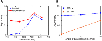
The transmission of light through sub-wavelength apertures (zero-mode waveguides, ZMW) in metal films is well-explored. It introduces both an amplitude modulation as well as a phase shift to the oscillating electromagnetic field. We propose a nanophotonic interferometer by bringing two ZMW (∼100 nm diameter) in proximity and monitoring the distribution of transmitted light in the back-focal plane of collecting microscope objective (1.3 N.A.). We demonstrate that both an asymmetry induced by the binding of a quantum dot in one of the two ZMW, as well as an asymmetry in ZMW diameter yield qualitatively similar transmission patterns. We find that the complex pattern can be quantified through a scalar measure of asymmetry along the symmetry axis of the aperture pair. In a combined experimental and computational exploration of detectors with differing ZMW diameters, we find that the scalar asymmetry is a monotonous function of the diameter difference of the two apertures, and that the scalar asymmetry measure is higher if the sample is slightly displaced from the focal plane of the collecting microscope objective. An optimization of the detector geometry determined that the maximum response is achieved at an aperture separation that is comparable to the wavelength on the exit side of the sensor. For small separations of apertures, on the order of a quarter of the wavelength and less, the signal is strongly polarization dependent, while for larger separations, on the order of the wavelength or larger, the signal becomes essentially polarization-independent.

Keywords: interferometer; sub-wavelength aperture; zero mode waveguide.


Figures

Figure 1.
Figure 1.
Structure of ZMW pair sensor. (A) Cross-section of device structure. (B) SEM of device region with four ZMW pair sensors. (C) Zoom of one pair in panel (B) with a 240 nm spacing, an average hole size of 105 nm, and a diameter difference of 15 nm.
Figure 2.
Figure 2.
Schematic of optical setup. The setup is a microscope in transmission mode which enables monitoring of the direction of the transmitted light through sample from an area that is selected by a pinhole.
Figure 3.
Figure 3.
Simulation setup showing the dimensions and variable definitions. S is the separation, D is the mean diameter, and Δ is the diameter difference.
Figure 4.
Figure 4.
Detection of single Q-Dot by ZMW pair. (A) Back-focal-plane half images at 820 nm illumination. Red frame (top): No exposure to Q-Dot. Blue frame (bottom): Exposure to Q-Dot. Scale bar is 0.4 mm. (B) Time-resolved fluorescence intensities (blue with Q-Dot, red no Q-Dot) recorded on focal-plane CCD under 520 nm illumination. (C) Intensity distribution along the horizontal axis in panel (A) that connect two holes (blue with Q-Dot, red no Q-Dot).
Figure 5.
Figure 5.
Transmitted intensity on back-focal CCD by pairs with 445 nm horizontal separation, mean hole diameter of 106 nm, and diameter difference of 12 nm with 820 nm horizontally-polarized illumination. (A) SEM image, scale bar 100 nm. (B) Experimental data, scale bar 0.3 mm. (C) Computed data. Scale bar 0.3 mm. (D) Experimental profile along horizontal cross section (labelled I in A). (E) Computed profile along horizontal cross section (labelled I in (B). (F) Experimental profile along vertical cross section (labelled II in A). G Computed profile along vertical cross section (labelled II in C).
Figure 6.
Figure 6.
Simulations of transmitted intensity profile on back-focal plane CCD by ZMW pairs with 400 nm separation. (A) Asymmetric pair with ZMW diameters of 80 nm and 100 nm. Scale bar is 0.3 mm on CCD chip. (B) Symmetric pair with equal diameters of 90 nm. Scale bar is 0.3 mm on CCD chip. (C) Cross-sections for asymmetric pair. Blue solid line with squares is profile along section I in panel (A). Red dashed line with circles is section II in panel (A). (D) Cross-sections for the symmetric pair. The solid line with squares is profile along section I in panel (B). Red dashed line with circles is section II in panel (B).
Figure 7.
Figure 7.
Patterns for large and small separations. (A) Back-focal profile from device with 620 nm spacing, mean diameter of 108 nm, and diameter difference of 13 nm. Scale bar is 1 mm. (B) Back-focal images of ZMW pair with 240 nm hole spacing, mean diameter of 105 nm, and diameter difference of 14 nm. Scale bar is 0.5 mm. (C) Section through A along the indicated line. (D) Section through B along the indicated line.
Figure 8.
Figure 8.
Focal plane images of ZMW pair with 650 nm hole spacing and an average hole diameter of 109 nm. (A) shows the experimental image for a diameter difference of 10 nm, while (B) shows the simulation for the same condition. (C) studies the intensity profile along the symmetry axis in the experimental data of panel A (indicated there as a dashed line) as well as diameter differences of 1 nm, 4 nm and 6 nm. (D) shows the intensity profile along the same axis in the simulated data of panel B and the other diameter differences.
Figure 9.
Figure 9.
Illustration of fitting of sections along symmetry axis for small and large separations. (A) Back-focal profile from device with 240 nm spacing, mean diameter of 105 nm, and diameter difference of 14 nm. The scalar asymmetry is 0.14. (B) Back-focal profile from device with 640 nm spacing, mean diameter of 102 nm, and diameter difference of 6 nm. The scalar asymmetry is 0.18. Dashed black lines are experimental data, blue lines are the composite fit, and red lines are the individual Gaussians that constitute the fit.
Figure 10.
Figure 10.
FDTD simulation of intensity distribution at the bottom of ZMW.
Figure 11.
Figure 11.
Evolution of axial profile of transmission pattern by a ZMW pair with separation of 650 nm, average hole diameter of 110 nm, and diameter difference of 10 nm for observation planes with numerical asymmetries indicated. (A) Back-focal CCD while sample is at focal point. (B) Focal CCD with best achievable focus. (C) Back-focal CCD while sample is displaced by +500 nm from focal point. (D) Back-focal CCD while sample is displaced by −500 nm from focal point.
Figure 12.
Figure 12.
Asymmetry versus hole diameter for devices with an approximate hole separation of 650 nm and an approximate mean hole diameter of 111 nm measured on the back-focal CCD with a +500 nm displacement of the sample from the microscope objective focal plane.
Figure 13.
Figure 13.
Test for asymmetries in transmission by collection optics. Panel (A) shows cross-section of back-focal CCD intensity as the same ZMW pair is rotated by 180° (separation of 640 nm, mean diameter of 110 nm, and diameter difference of 10 nm). Panel (B) shows show cross-section of back-focal CCD intensity of two different ZMW on the same wafer that have symmetry axes that are perpendicular to each other (separation of 640 nm, mean diameter 102 nm, diameter difference 6 nm). The polarization of the incident beam was parallel to the symmetry axis.
Figure 14.
Figure 14.
Measured asymmetry as function of hole separation and polarization for ZMW pairs with an approximate mean diameter of 110 nm and approximate diameter difference of 13 nm. (A) Experimentally measured asymmetries on the back-focal CCD. Blue squares are for polarization parallel to the pair axis, and red diamonds are for polarization perpendicular to the pair axis. (B) Comparison of the angular dependence of the scalar asymmetry measure for the large spacing (523 nm separation, 103 nm mean diameter, 14 nm diameter difference, blue squares) and small spacing (237 nm separation, 105 nm mean diameter, 14 nm diameter difference, red diamonds) devices.
Figure 15.
Figure 15.
Computed asymmetries as function of hole separation and polarization for ZMW pairs with an approximate mean diameter of 110 nm, approximate diameter difference of 13 nm, and polarization parallel to the symmetry axis.

References

    1. Arroyo J O, Kukura P. Non-fluorescent schemes for single-molecule detection, imaging and spectroscopy. Nat. Photon. 2016;10:11–7. doi: 10.1038/nphoton.2015.251. - DOI
    1. Born M, Wolf E. Principles of Optics. Cambridge: Cambridge University Press; 2019.
    1. Sriram M, Zong K, Vivekchand S R C, Justin Gooding J. Single nanoparticle plasmonic sensors. Sensors (Switzerland) 2015;15:25774–92. doi: 10.3390/s151025774. - DOI - PMC - PubMed
    1. Haes A J, Van Duyne R P. A nanoscale optical biosensor: sensitivity and selectivity of an approach based on the localized surface plasmon resonance spectroscopy of triangular silver nanoparticles. J. Am. Chem. Soc. 2002;124:10596–604. doi: 10.1021/ja020393x. - DOI - PubMed
    1. Baaske M D, Foreman M R, Vollmer F. Single-molecule nucleic acid interactions monitored on a label-free microcavity biosensor platform. Nat. Nanotechnol. 2014;9:933–9. doi: 10.1038/nnano.2014.180. - DOI - PubMed

LinkOut - more resources