

A Microscale 3D Printing Based on the Electric-Field-Driven Jet
- PMID: 36654877
- PMCID: PMC9586217
- DOI: 10.1089/3dp.2018.0154
A Microscale 3D Printing Based on the Electric-Field-Driven Jet
Abstract
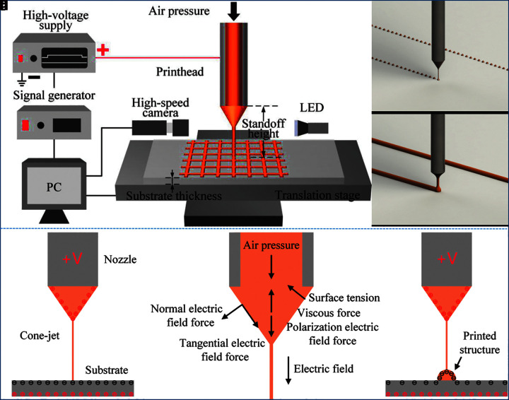
This study presents a novel microscale three-dimensional (3D) printing based on the electric-field-driven (EFD) jet. Differing from the traditional electrohydrodynamic jet printing with two counter electrodes, the EFD jet 3D printing forms electric field between the nozzle electrode and the top surface of the substrate or printed structure only using a single potential by the nozzle electrode. The numerical simulations and experimental studies were carried out to verify the capabilities and advantages of the proposed approach, which includes the suitability of substrates, the potentials of the conformal printing, and the large size 3D printing. Besides, considering the high-resolution and high-efficiency printing of various materials with different viscosities, two working modes, including the pulsed cone-jet mode and the continuous cone-jet mode, were proposed and investigated by the CCD camera. Finally, several typical printed structures were provided to demonstrate the feasibility of the proposed technology for microscale two-dimensional patterning and macro/micro-3D structure fabrication. As a conclusion, this breakthrough technique provides a high-efficiency and high-resolution 3D printing technique enabling direct-write, noncontact, and additive patterning at microscale for a variety of ink systems and melted polymer materials, especially for the multiscale and multimaterial additive manufacturing.
Keywords: 3D printing; electric-field-driven; multimaterial; multiscale.
Copyright 2020, Mary Ann Liebert, Inc., publishers.
Conflict of interest statement
No competing financial interests exist.
Figures


Similar articles
-
Fabrication of a Large-Area, Fused Polymer Micromold Based on Electric-Field-Driven (EFD) μ-3D Printing.Polymers (Basel). 2019 Nov 18;11(11):1902. doi: 10.3390/polym11111902. Polymers (Basel). 2019. PMID: 31752165 Free PMC article.
-
Transient charge-driven 3D conformal printing via pulsed-plasma impingement.Proc Natl Acad Sci U S A. 2024 May 28;121(22):e2402135121. doi: 10.1073/pnas.2402135121. Epub 2024 May 21. Proc Natl Acad Sci U S A. 2024. PMID: 38771869 Free PMC article.
-
Directly Printed Embedded Metal Mesh for Flexible Transparent Electrode via Liquid Substrate Electric-Field-Driven Jet.Adv Sci (Weinh). 2022 May;9(14):e2105331. doi: 10.1002/advs.202105331. Epub 2022 Mar 1. Adv Sci (Weinh). 2022. PMID: 35233960 Free PMC article.
-
Micro/nanoscale electrohydrodynamic printing: from 2D to 3D.Nanoscale. 2016 Aug 25;8(34):15376-88. doi: 10.1039/c6nr04106j. Nanoscale. 2016. PMID: 27479715 Review.
-
Toward Multiscale, Multimaterial 3D Printing.Adv Mater. 2024 Aug;36(34):e2314204. doi: 10.1002/adma.202314204. Epub 2024 Jun 4. Adv Mater. 2024. PMID: 38775924 Review.
Cited by
-
Recent Advances in Design and Preparation of Polymer-Based Thermal Management Material.Polymers (Basel). 2021 Aug 20;13(16):2797. doi: 10.3390/polym13162797. Polymers (Basel). 2021. PMID: 34451339 Free PMC article. Review.
-
The Electric-Field-Driven Fusion Jetting 3D Printing for Fabricating High Resolution Polylactic Acid/Multi-Walled Carbon Nanotube Composite Micro-Scale Structures.Micromachines (Basel). 2020 Dec 21;11(12):1132. doi: 10.3390/mi11121132. Micromachines (Basel). 2020. PMID: 33371443 Free PMC article.
-
Facile Adaptation of a Fused Deposition Modeling 3D Printer to Motionless Printing through Programmable Electric Relay: Discretized Modeling and Experiments.3D Print Addit Manuf. 2024 Feb 1;11(1):251-260. doi: 10.1089/3dp.2022.0062. Epub 2024 Feb 15. 3D Print Addit Manuf. 2024. PMID: 38389683 Free PMC article.
-
Electric-Field-Driven Printed 3D Highly Ordered Microstructure with Cell Feature Size Promotes the Maturation of Engineered Cardiac Tissues.Adv Sci (Weinh). 2023 Apr;10(11):e2206264. doi: 10.1002/advs.202206264. Epub 2023 Feb 13. Adv Sci (Weinh). 2023. PMID: 36782337 Free PMC article.
-
Directly printed standing ceramic circuit boards for rapid prototyping of miniaturization and high-power of electronics.Nat Commun. 2025 Jun 6;16(1):5258. doi: 10.1038/s41467-025-60408-x. Nat Commun. 2025. PMID: 40480979 Free PMC article.
References
-
- Zhang B, He J, Li X, et al. . Micro/nanoscale electrohydrodynamic printing: From 2D to 3D. Nanoscale 2016;8:15376. - PubMed
-
- Lifton VA, Lifton G, Simon S. Options for additive rapid prototyping methods (3D printing) in MEMS technology. Rapid Prototyp J 2014;20:403–412.
-
- Du X, Chen Z, Li Z, et al. . Dip-coated gold nanoparticle electrodes for aqueous-solution-processed large-area solar cells. Adv Energy Mater 2014;4:105–110.
-
- Cohen A, Chen R, Frodis U, et al. . Microscale metal additive manufacturing of multi-component medical devices. Rapid Prototyp J 2010;16:209–215.
-
- Ciocci M, Mochi F, Carotenuto F, et al. . Scaffold-in-scaffold potential to induce growth and differentiation of cardiac progenitor cells. Stem Cells Dev 2017;26. - PubMed
LinkOut - more resources
Full Text Sources
Research Materials