Review
. 2023 Feb 20;52(4):1288-1330.
doi: 10.1039/d2cs00570k.

Antimonene: a tuneable post-graphene material for advanced applications in optoelectronics, catalysis, energy and biomedicine

Affiliations
Review

Antimonene: a tuneable post-graphene material for advanced applications in optoelectronics, catalysis, energy and biomedicine

Jose A Carrasco et al. Chem Soc Rev. .

Abstract

The post-graphene era is undoubtedly marked by two-dimensional (2D) materials such as quasi-van der Waals antimonene. This emerging material has a fascinating structure, exhibits a pronounced chemical reactivity (in contrast to graphene), possesses outstanding electronic properties and has been postulated for a plethora of applications. However, chemistry and physics of antimonene remain in their infancy, but fortunately recent discoveries have shed light on its unmatched allotropy and rich chemical reactivity offering a myriad of unprecedented possibilities in terms of fundamental studies and applications. Indeed, antimonene can be considered as one of the most appealing post-graphene 2D materials reported to date, since its structure, properties and applications can be chemically engineered from the ground up (both using top-down and bottom-up approaches), offering an unprecedented level of control in the realm of 2D materials. In this review, we provide an in-depth analysis of the recent advances in the synthesis, characterization and applications of antimonene. First, we start with a general introduction to antimonene, and then we focus on its general chemistry, physical properties, characterization and synthetic strategies. We then perform a comprehensive study on the allotropy, the phase transition mechanisms, the oxidation behaviour and chemical functionalization. From a technological point of view, we further discuss the applications recently reported for antimonene in the fields of optoelectronics, catalysis, energy storage, cancer therapy and sensing. Finally, important aspects such as new scalable methodologies or the promising perspectives in biomedicine are discussed, pinpointing antimonene as a cutting-edge material of broad interest for researchers working in chemistry, physics, materials science and biomedicine.


Conflict of interest statement

There are no conflicts to declare.

Figures

Scheme 1
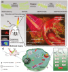
Scheme 1. Summary of antimonene synthesis and applications. The image above represents (top) the synthesis of antimonene from bulk antimony or via the assembly of antimony atoms on a substrate and (bottom) the applications of antimonene as a multifunctional material. From left to right: optoelectronic devices, solar cells, catalysis, field-effect transistors, energy storage, biomedical applications by binding molecules of interest and destroying carcinogenic cells.
Fig. 1
Fig. 1. Schematic representation of the production of elemental antimony from stibnite. Adapted from ref. with permission from John Wiley & Sons, copyright 2011.
Fig. 2
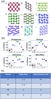
Fig. 2. (a) Typical honeycomb and non-honeycomb structures of 2D pnictogen allotropes. (b) Average binding energies of the different allotropes, highlighting the β phase as the most stable in average. (c) Table summarizing the stable phases of the different pnictogens. While α phase presents a parallel puckered layer with space group of Cmca, β phase exhibits parallel buckled layers with the Rm space group in a rhombohedral structure. Adapted from ref. with permission from Royal Society of Chemistry, copyright 2018.
Fig. 3
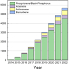
Fig. 3. Graphic showing the cumulative number of papers focused on 2D pnictogens. Data acquired from Scopus on October 2022.
Fig. 4
Fig. 4. Building van der Waals heterostructures by combining different layers of 2D materials. Adapted from ref. .
Fig. 5
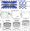
Fig. 5. Crystal structure and band structure of few-layer phosphorene. (a) Perspective side view of few-layer phosphorene. (b) and (c) Side and top views of few-layer phosphorene. (d) Theoretical band structure of a phosphorene monolayer calculated using DFT-HSE06. (e) and (f) DFT-HSE06 results for the dependence of the energy gap in few-layer phosphorene on (e) the number of layers and (f) the strain along the x- and y-directions in a monolayer system. (g) Representation of the electronic band structures of antimony trilayers, bilayers, and monolayers calculated using DFT-HSE06. Adapted from ref. with permission from American Chemical Society, copyright 2014 and ref. with permission from John Wiley & Sons, copyright 2015.
Fig. 6
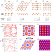
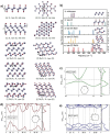
Fig. 6. Top: Structural configurations of antimonene allotropes: (a) α-Sb, (b) β-Sb, (c) γ-Sb, and (d) δ-Sb. Bottom: Electronic properties of (a)–(c) α-Sb and (d)–(f) β-Sb monolayers: (a), (d) band structure, (b), (e) charge density projected in the plane, and (c), (f) simulated scanning tunneling microscopy (STM) images. Adapted from ref. with permission from American Chemical Society, copyright 2015.
Fig. 7
Fig. 7. (a) Step-by-step procedure (1–8) for the exfoliation of ANSs using micromechanical approach. Inset in (8) Optical micrographs showing exfoliated ANSs with different polygonal geometries. Scale bars 20 μm. (b) AFM image of typical ANSs and (c) height profiles along the dashed lines showing steps of approximately 1 nm, compatible with a single layer antimonene. Adapted from ref. with permission from IOP Publishing, copyright 2020.
Fig. 8
Fig. 8. (a) The lattice thermal conductivity of antimonene as a function of temperature. (b) Zenith view of the temperature mapping for a rectangular flake (white lines) considering a disk-like heat source (black circle). (c) Average temperature of the excitation spot as a function of the heat source rate for different thermal conductivities of the flake. (d) Temperature of the probed ANS as a function of laser power, estimated using both calculated power and temperature coefficients. Adapted from ref. with permission from Royal Society of Chemistry, copyright 2016, and ref. with permission from IOP Publishing, copyright 2020.
Fig. 9
Fig. 9. Main synthetic approaches in the synthesis of antimonene classified in top-down and bottom-up approaches. Acronyms stand for mechanical exfoliation (ME), liquid phase exfoliation (LPE), electrochemical exfoliation (EE), epitaxial growth (EG) and solution-phase synthesis (SPS).
Fig. 10
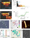
Fig. 10. AFM topography images of an antimonene flake with a monolayer terrace at the bottom. (a) AFM topography showing an antimonene flake with terraces of different heights. (b) Height histogram of the image in (a) pointing out the different thicknesses of the terraces. (c) Same flake as in (a) after a nanomanipulation process to confirm the stability of the material. The lower terrace of the flake was folded upward resulting in an origami structure with different folds. The inset corresponds to the area of the origami where the lowest step height is found. (d) Profile along the green line in the inset in (c). (e) Optical micrograph of a typical antimonene nanosheet isolated on SiO2/Si substrate using micromechanical exfoliation. (f) False-colored AFM image of the same ANSs with incremental color code to highlight the terraces. Each color indicates a 10 nm step (g) AFM image of a few-layer antimonene nanosheet and height profile along the dashed yellow line. (h) Comparative Raman spectra of the pristine bulk (100 nm) and few-layer (14 nm) antimonene nanosheets, remarking the blue shift of the of A1g and Eg modes for the few-layer antimonene nanosheets. (i) Scanning Raman microscopy (SRM) map of the intensity of A1g mode of the flakes in (e). (j) Scanning electron microscope (SEM) image of the same flakes in (e). Adapted from ref. with permission from John Wiley & Sons, copyright 2016, and ref. with permission from IOP Publishing, copyright 2020.
Fig. 11
Fig. 11. (a) TEM image of FL antimonene nanolayers. (b) Representative topographic AFM image (scale bar 2 μm) of the exfoliated FL antimonene nanolayers. (c) Corresponding Raman A1g map (scale bar 2 μm) of the exfoliated FL antimonene nanolayers contained in the area dotted in white in (b). (d) AFM image of typical ANS showing polydisperse nanosheets exfoliated by ultrasonication. (e) Statistical dispersion of ANS lateral size as a function of thickness. (f) Thickness measured by AFM along the lines numbered in (d). Adapted from ref. with permission from Royal Society of Chemistry, copyright 2019, and ref. with permission from IOP Publishing, copyright 2020.
Fig. 12
Fig. 12. (a) Fabrication of PEG-coated AMQDs. (b) Images of bulk antimony, antimony powder, and AMQD solution during the preparation process. (c) TEM image, (d) diameter distribution, (e) AFM image, and (f) thickness of the PEG-coated AMQDs. (g) FTIR spectrum, (h) Raman spectrum, and (i) XRD spectrum of AMQDs and PEG-coated AMQDs. Reproduced from ref. with permission from John Wiley & Sons, copyright 2017.
Fig. 13
Fig. 13. Characterization of the prepared multilayer antimonene by electrochemical exfoliation. (a) Schematic illustration of the two-electrode system used for the procedure, depicting bulk Sb, Pt wire, and Na2SO4 aqueous solution as the working electrode, counter electrode, and electrolyte, respectively. (b) AFM image of a multilayer antimonene nanoflake obtained by electrochemical exfoliation. (c), (d) TEM and HRTEM images of the electrochemical exfoliated antimonene. (e) Raman spectra of the bulk antimony and multilayer antimonene shown in (b). (f) XPS spectrum showing the Sb 3d5/2 peak of the exfoliated multilayer antimonene. Reproduced from ref. with permission from John Wiley & Sons, copyright 2017.
Fig. 14
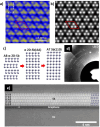
Fig. 14. Top: (a) Schematic of fabrication of an antimonene monolayer formed on the PdTe2 substrate obtained by MBE approach. (b) STM topographic image of large antimonene island on PdTe2. (Inset: LEED pattern of antimonene on PdTe2.) (c) Atomic resolution STM image of monolayer antimonene showing the graphene-like honeycomb structure. (d) Top view and side view of the buckled conformation of the antimonene honeycomb. (e) Height profile along the red line in (b), showing that the apparent height of the antimonene island is 2.8 Å. (f) Line profile corresponding to the blue line in (c), revealing the periodicity of the antimonene lattice (4.13 ± 0.02 Å). Bottom: (a) Schematic of the MBE fabrication process. (b) LEED pattern of a clean Ag(111) substrate. (c) LEED pattern of antimonene on Ag(111). (d) Large scale STM image of monolayer antimonene on the Ag(111) (inset: height profile along the yellow line at the terrace edge). (e) High-resolution STM image of antimonene depicted by the white square in (d). (f) Line profile corresponding to the red line in (e), revealing the periodicity of the antimonene lattice (5.01 Å). Adapted from ref. with permission from John Wiley & Sons, copyright 2016, and ref. with permission from American Chemical Society, copyright 2018.
Fig. 15
Fig. 15. Antimonene synthesized on mica substrates via vdW epitaxy. (a) Schematic illustration of the sample synthesis configurations. (b) Schematic diagram of the vdWE. (c)–(f) Optical images of typical antimonene polygons with triangular, hexagonal, rhombic, and trapezoidal shapes, respectively. The scale bar is 5 mm. (g) AFM image of a typical triangular antimonene sheet. The scale bar is 1 mm. (h) AFM image of a tiny antimonene sheet with a thickness of ca. 1 nm. The scale bar is 50 nm. Reproduced from ref. with permission from Springer Nature, copyright 2016.
Fig. 16
Fig. 16. Top: Illustration of the wet chemical solution-phase synthesis of antimony trioxide, antimony tetrahedral, and hexagonal antimonene nanosheets from Sb-oleate, Sb(OAc)3-DDT, and SbCl3-DDT as precursors, respectively. Bottom: AFM images and the corresponding height profiles of hexagonal antimonene nanosheets with tunable layer thicknesses obtained at different annealing times at 300 °C: (a) 10 s, (b) 30 s, (c) 60 s, and (d) 120 s. Reproduced from ref. with permission from John Wiley & Sons, copyright 2019.
Fig. 17
Fig. 17. Main approaches in solution-phase synthesis of antimonene hexagons. Above: Schematic representation of hot injection method and parameters influencing the outcome of the synthesis. Below: Illustration of the continuous-flow reactor. On the right, different characterization performed in the obtained antimonene hexagons from the optimized solution-phase synthesis of antimonene: (a) AFM, (b) Raman mapping and (c) Raman spectra, (d) XPS, (e) HAADF STEM and (f) Colorized HAADF STEM, inset showing the fast Fourier transformation. (g)–(i) Elemental compositional EELS maps. Scale bar (e)–(i) 100 nm. Adapted from ref. with permission from John Wiley & Sons, copyright 2021.
Fig. 18
Fig. 18. Timeline highlighting the development of the different synthetic approaches to obtain antimonene.
Fig. 19
Fig. 19. (a) Atomically resolved STM image of an antimonene monolayer on SbAg2 surface alloy on Ag(111). (b) The simulated STM in the constant height mode (∼2 Å). (c) Schematic representation of the layer-dependent A17 (AB α-2D-Sb) transition to A7 in antimonene. (d) LEED pattern of 2D-Sb on graphene. Part of the Ewald sphere at 44 eV is shown in the bottom left and at 29 eV is shown in the top right. (e) STEM of a cross section of 4 bilayers A17 antimonene island on graphene. Adapted from ref. and with permission from American Chemical Society, copyright 2020.
Fig. 20
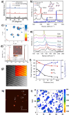
Fig. 20. (a) X-ray diffraction (XRD) patterns of bulk antimony crystals, antimony plates after ball-milling and antimonene. (b) Raman spectra of bulk antimony (β-phase), few-layer antimonene and antimony trioxide. Inset: Vibrational modes of β-phase antimonene. (c) A1g intensity Raman mapping of solvent-exfoliated flakes deposited on a SiO2/Si substrate. (d) Single-point Raman spectra measured at different thicknesses according to the topographic AFM image (inset) of the same area studied in (c) (dashed lines). (e) Raman spectra of antimonene polygons with different thicknesses, from 5 nm to bulk. (f) A1g, Eg peak frequencies and energy difference of those two peaks plotted against sample thickness. (g) Atomic resolution HAADF image acquired on the edge of a free-standing portion of an antimonene flake obtained by LPE. The scale bar is 2 nm. (h) Representative AFM topography image (scale bar 5 μm) of exfoliated antimonene onto SiO2/Si substrates. (i) The corresponding Raman A1g mapping of the same antimonene flakes in (h). Adapted from ref. and with permission from Springer Nature, copyright 2019 and 2016, ref. with permission from John Wiley & Sons, copyright 2016, and ref. with permission from the Royal Society of Chemistry, copyright 2020.
Fig. 21
Fig. 21. (a) Raman spectra of bulk antimony, exfoliated ANS and oxidized-ANS exhibiting Sb2O3 Raman fingerprint at 254.6 cm−1. (b) HAADF image of sub-nanometric ANS acquired at 80 kV and the corresponding elemental compositional maps derived from EELS. (c) High-magnification annular bright field (ABF) image near the edge of the nanosheet displayed in (b) (orange-dashed area) (scale bar 5 nm). (d) XPS line spectra in the Sb 3d region for antimonene nanosheet samples, as-exfoliated (left column) and after thermal annealing at 210 °C under high vacuum (right column). (e) VEELS spectrum of the β-Sb(001) crystal on suspended graphene (ADF STEM in the inset). Spectrum acquired after ∼8 months ambient air exposure of the sample. (f) Atomic model of the suggested Sb2O3(111) formed from ambient air exposure on β-Sb(001) crystals. Adapted from ref. with permission from Springer Nature, copyright 2021, and ref. with permission from IOP Publishing, copyright 2020.
Fig. 22
Fig. 22. Left: (a) Sb 3d image for the reference sample. Letters refer to the antimonene flakes studied. (b) Sb 3d peak for the reference sample, corresponding to point B in (a). Numbers identify the different components: 1 (Sb 3d5/2), 2 (oxidized Sb 3d5/2), and 3 (O 1s). Peaks at higher BEs are the Sb 3d3/2 components. (c) The Sb 3d image for the functionalized antimonene. (d) Sb 3d peak for the functionalized sample, corresponding to point E in (c). The peak identification and other details are as in (b). The size of images in (a) and (c) is 40 × 40 μm. Right: XPS Sb 3d and O 1s region of the neat bmim-BF4 IL (I) showing oxygen signals from the IL surface contamination layer, of the highly-concentrated FL-Sb suspension (II) showing small signals of non-oxidized (Sb 3d5/2 at 528.2 eV) and minor contributions from oxidized (530.3 eV) antimony next to the oxygen contamination, after removal of most of the IL by heating in UHV (III), and after submitting the sample to environmental conditions for a day, showing a drastic decrease in Sb(0). Adapted from ref. with permission from Springer Nature, copyright 2019, and ref. with permission from John Wiley & Sons, copyright 2017.
Fig. 23
Fig. 23. (a) Type (I) antimonene oxide structures with one layer in side view (a) and top view (b), and two layers in (c) and (d). Type (II) antimonene oxide heterostructures with different stoichiometries of the oxidized layers: (e) and (f) Sb2O; (g) and (h) Sb2O2; and (i) and (j) Sb2O3. Type (II) structures in the top view show the oxidized layer only. Oxygen (antimony) atoms are shown in red (gray). Labels a and b on the figures indicate the in-plane lattice vectors. (b) Calculated frequencies of Raman-active vibrational modes in (1) antimonene, (2) type (I), (3)–(5) type (II) antimonene oxide structures1.(c)–(e) Electronic band structures and density of states calculated using the hybrid functional HSE12 and inclusion of spin–orbit interactions (SOI) for (c) type (I) Sb2O2, (d) type (II) Sb2O2, and (e) type (II) Sb2O3 monolayers. Gray dashed lines are the results without SOI and are almost congruent with the bands with SOI for (c) and (d). The zero of energy is set to the Fermi energy. Adapted from ref. with permission from American Physical Society, copyright 2022.
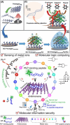
Fig. 24
Fig. 24. Atomic structure of 2D Sb2O3 molecular crystals. (a), (b) Top-view structural models of monolayer and trilayer Sb2O3 flakes with the (111) plane. Brown balls, Sb atoms. Red balls, O atoms. (c) TEM image of a triangular Sb2O3 flake. (d) SAED pattern of the Sb2O3 flake. (e) Z-contrast atomic-level HAADF-STEM image of the Sb2O3 flake showing the perfect atomic lattice. (f) Enlarged HAADF image and the matched atomic ball model, white atoms are marked by yellow circles and gray atoms are marked by blue circles. (g) Scattered electron intensity color image for (f). (h) Intensity line profile along the red box in (g). (i)–(k) HAADF image of a stacked flake and the corresponding elemental maps for Sb and O. (l) EDX and EELS spectra of the Sb2O3 flake. Reproduced from ref. with permission from Springer Nature, copyright 2019.
Fig. 25
Fig. 25. Top: (a) Structure of β-antimonene (top panel) and the perylene bisimide (PDI) molecule (bottom panel). (b) AFM topographic images showing an antimonene flake of about 10 nm of thickness. Top: Flake as deposited. Middle: Same flake after the functionalization with PDI molecules. Bottom: Height histograms of the flake before (green) and after functionalization (blue), showing an average thickness increase of 4.1 nm. The average PDI coverage in all the studied flakes was 3.6 nm. The inset shows representative profiles corresponding to the lines in the images. (c) Scanning Raman microscopy (SRM) of the same flake. Left: Silicon intensity Raman map showing a decrease in the 521 cm−1 signal which clearly reveals the morphology of the flake. Right: Raman intensity mapping shows the exclusive self-assembly of the PDI on the antimonene flakes and not on the Si/SiO2 substrate. (d) Mean Raman spectra (excitation at 532 nm) of the flake showing the PDI bands as a consequence of the quenching of its fluorescence. Bottom: Formation and electrophoretic depositions of FLSb-C60 composite clusters. Adapted from ref. and with permission from John Wiley & Sons, copyright 2017 and 2020.
Fig. 26
Fig. 26. Top, schematic illustration of the experimental setup for the electrochemical exfoliation and synchronous halogenation of antimonene in an ionic liquid-based electrolyte. Bottom, schematic illustration for the preparation of silane-functionalized antimonene nanosheets and their copolymerized gel glasses. Adapted from ref. with permission from John Wiley & Sons, copyright 2019 and ref. with permission from American Chemical Society, copyright 2021.
Fig. 27
Fig. 27. Top: (a) Comparison of energy levels of each functional layer. The Fermi level of antimonene is represented by the dashed line. (b) Configuration of the antimonene-based device. (c) Cross-sectional SEM image of the studied device. (d) Current-density–voltage (J–V) curves of devices with different architectures. (e) External quantum efficiency (EQE) spectra together with EQE-data-based integrated short-circuit current densities (Jsc) for devices 1 (HTL-free) and 2 (ITO/antimonene/perovskite/PCBM/Bphen/Al). Bottom: Device structure and performance characterization of an antimonene organic-photovoltaics device. (a) Device architecture including the AMQSs. (b) Band structure of the organic-photovoltaics device. (c) Current density–voltage (JV) curves and (d) EQE characteristics of the best reference device and the devices with different concentrations of AMQDs in their active layer. Adapted from ref. with permission from John Wiley & Sons, copyright 2018, and ref. with permission from the Royal Society of Chemistry, copyright 2018.
Fig. 28
Fig. 28. (a) LSV curves of the different FL antimonene samples, Nafion modified glassy carbon blank and platinum blank. (b) Tafel slope values and (c) overpotentials required for 10 mA cm−2 calculated from LSV data. CV curves recorded after LSV measurements of (d) Sb-BuOH and (e) Sb-NMP. CV curves recorded before LSV measurements of the (f) Sb-BuOH and (g) Sb-NMP samples. (h) Voltammograms obtained between −0.9 V and different anodic potential limits measured using 50 mV s−1. (i) Voltammograms obtained between 0.5 V and different cathodic potential limits measured using 50 mV s−1. The insets show the calculated charges obtained when a positive current is passed (Qox) or negative current is passed (Qred). Adapted from ref. with permission from Royal Society of Chemistry, copyright 2018.
Fig. 29
Fig. 29. Mechanistic studies. Experimental evidence and proposed mechanisms for few-layer black phosphorus (FL-Bp), FL-Sb, and superacid triflic acid (HOTf) catalyzed alkylation of nucleophiles with esters in bmim-BF4. Reproduced from ref. with permission from Springer Nature, copyright 2019.
Fig. 30
Fig. 30. Schematic illustration of the proposed discharge–charge mechanism for the Sb–C framework film anodes as the high-performance sodium battery with unusual reversible crystalline-phase transformation. Reproduced from ref. with permission from American Chemical Society, copyright 2016.
Fig. 31
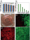
Fig. 31. (a) Cell viability after incubation with only PEG-coated AMQDs. (b) Cell viability of MCF-7 cells treated with PEG-coated AMQDs with NIR (808 nm, 1 W cm−2) for 5 minutes. (c) A photo of the cell culture dish after incubation with PEG-coated AMQDs. The black circle with shadow shows the laser spot. (d)–(f) Confocal images of calcein antimonene (green, live cells) and propidium iodide (PI) (red, dead cells) co-stained MCF-7 cells after exposure to NIR irradiation (808 nm, 1 W cm−2). The amplification of confocal images is 100×. Reproduced from ref. with permission from John Wiley & Sons, copyright 2017.
Fig. 32
Fig. 32. Schematic illustration of (a) the preparation of 2D antimonene-PEG-doxorubicin nanosheets and (b) their administration as photonic nanomedicines for cancer theranostics, (c) Nanopoxia treatment and methods of action. Adapted from ref. and with permission from John Wiley & Sons, copyright 2018 and 2020.
Fig. 33
Fig. 33. Top (a) Shear exfoliated pnictogens using a kitchen blender. (b) Biosensor preparation using layer-by-layer drop-cast pnictogen nanosheets, tyrosinase (Tyr), and glutaraldehyde (Glu) onto a glassy carbon (GC) electrode. (c) Chemical mechanism of phenol detection by a biosensor based on exfoliated pnictogen and Tyr. Bottom, scheme of a peptide fluorescence sensing system using antimonene and its different applications in the detection of Pb2+, molecular logic operations and crypto-steganography. Adapted from ref. with permission from John Wiley & Sons, copyright 2019, and ref. with permission from American Chemical Society, copyright 2022.
None
Jose A. Carrasco
None
Pau Congost-Escoin
None
Mhamed Assebban
None
Gonzalo Abellán

References

    1. Fiori G. Bonaccorso F. Iannaccone G. Palacios T. Neumaier D. Seabaugh A. Banerjee S. K. Colombo L. Electronics Based on Two-Dimensional Materials. Nat. Nanotechnol. 2014;9(10):768–779. doi: 10.1038/nnano.2014.207. doi: 10.1038/nnano.2014.207. - DOI - DOI - PubMed
    1. Zhang Y. Rubio A. Lay G. L. Emergent Elemental Two-Dimensional Materials beyond Graphene. J. Phys. D: Appl. Phys. 2017;50(5):053004. doi: 10.1088/1361-6463/aa4e8b. doi: 10.1088/1361-6463/aa4e8b. - DOI - DOI
    1. Glavin N. R. Rao R. Varshney V. Bianco E. Apte A. Roy A. Ringe E. Ajayan P. M. Emerging Applications of Elemental 2D Materials. Adv. Mater. 2020;32(7):1904302. doi: 10.1002/adma.201904302. doi: 10.1002/adma.201904302. - DOI - DOI - PubMed
    1. Butler S. Z. Hollen S. M. Cao L. Cui Y. Gupta J. A. Gutiérrez H. R. Heinz T. F. Hong S. S. Huang J. Ismach A. F. Johnston-Halperin E. Kuno M. Plashnitsa V. V. Robinson R. D. Ruoff R. S. Salahuddin S. Shan J. Shi L. Spencer M. G. Terrones M. Windl W. Goldberger J. E. Progress, Challenges, and Opportunities in Two-Dimensional Materials Beyond Graphene. ACS Nano. 2013;7(4):2898–2926. doi: 10.1021/nn400280c. doi: 10.1021/nn400280c. - DOI - DOI - PubMed
    1. Geng D. Yang H. Y. Recent Advances in Growth of Novel 2D Materials: Beyond Graphene and Transition Metal Dichalcogenides. Adv. Mater. 2018;30(45):1800865. doi: 10.1002/adma.201800865. doi: 10.1002/adma.201800865. - DOI - DOI - PubMed