

Selective electrodeposition of indium microstructures on silicon and their conversion into InAs and InSb semiconductors
- PMID: 36746886
- PMCID: PMC9902586
- DOI: 10.1186/s11671-023-03778-9
Selective electrodeposition of indium microstructures on silicon and their conversion into InAs and InSb semiconductors
Abstract
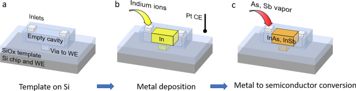
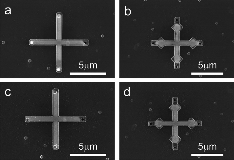
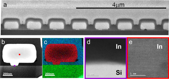
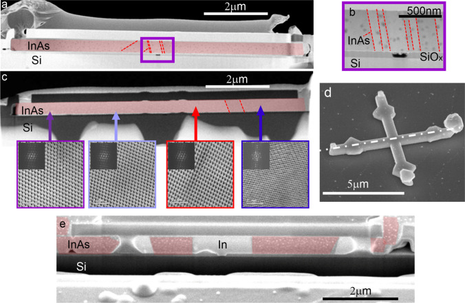
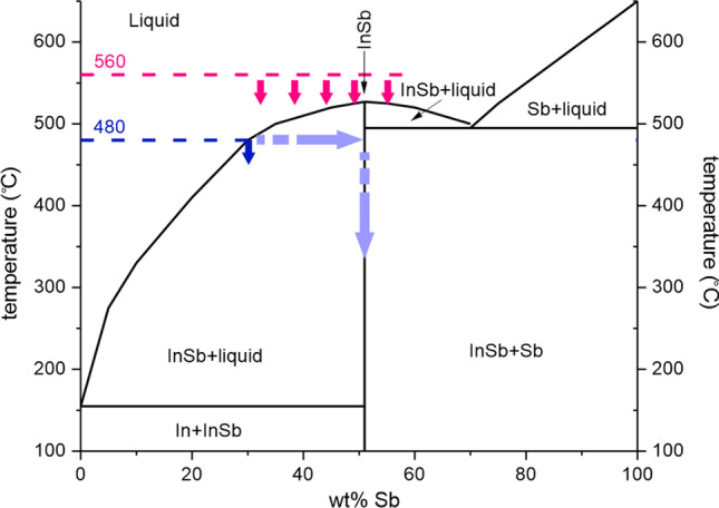
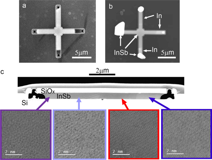
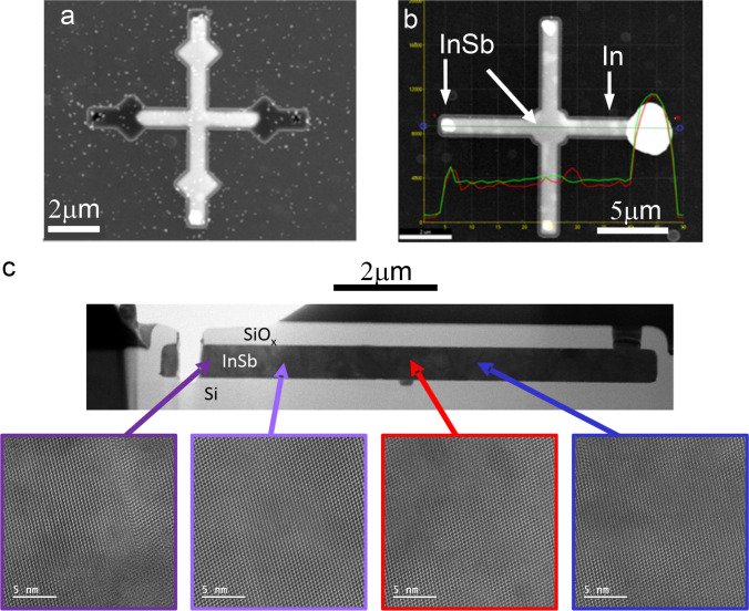
The idea of benefitting from the properties of III-V semiconductors and silicon on the same substrate has been occupying the minds of scientists for several years. Although the principle of III-V integration on a silicon-based platform is simple, it is often challenging to perform due to demanding requirements for sample preparation rising from a mismatch in physical properties between those semiconductor groups (e.g. different lattice constants and thermal expansion coefficients), high cost of device-grade materials formation and their post-processing. In this paper, we demonstrate the deposition of group-III metal and III-V semiconductors in microfabricated template structures on silicon as a strategy for heterogeneous device integration on Si. The metal (indium) is selectively electrodeposited in a 2-electrode galvanostatic configuration with the working electrode (WE) located in each template, resulting in well-defined In structures of high purity. The semiconductors InAs and InSb are obtained by vapour phase diffusion of the corresponding group-V element (As, Sb) into the liquified In confined in the template. We discuss in detail the morphological and structural characterization of the synthesized In, InAs and InSb crystals as well as chemical analysis through scanning electron microscopy (SEM), scanning transmission electron microscopy (TEM/STEM), and energy-dispersive X-ray spectroscopy (EDX). The proposed integration path combines the advantage of the mature top-down lithography technology to define device geometries and employs economic electrodeposition (ED) and vapour phase processes to directly integrate difficult-to-process materials on a silicon platform.
Keywords: Electrodeposition; III-Vs; Integration; Recrystallization; Saturation; TASE.
© 2023. The Author(s).
Conflict of interest statement
The authors have no conflicts of interest to declare that are relevant to the content of this article.
Figures
References
-
- Oskam G, Long JG, Natarajan A, Searson PC. Electrochemical deposition of metals onto silicon. J Phys D Appl Phys. 1998;31:1927–1949. doi: 10.1088/0022-3727/31/16/001. - DOI
-
- Elfadill NG, Hashim MR, Thabit KATh. The role of using seed-layer assisted electrodeposition method on the growth and the photovoltaic properties of p-Cu2O/n-Si heterojunctions. J Mater Sci Mater Electron. 2015;26:985–991. doi: 10.1007/s10854-014-2493-y. - DOI
-
- Dalchiele EA, Giorgi P, Marotti RE, et al. Electrodeposition of ZnO thin films on n-Si(100) Sol Energy Mater Sol Cells. 2001;70:245–254. doi: 10.1016/S0927-0248(01)00065-4. - DOI
-
- Al-Heuseen K, Hashim MR. One-step synthesis of GaN thin films on Si substrate by a convenient electrochemical technique at low temperature for different durations. J Cryst Growth. 2011;324:274–277. doi: 10.1016/j.jcrysgro.2011.03.051. - DOI
Grants and funding
LinkOut - more resources
Full Text Sources
Research Materials