. 2023 Feb 6;14(1):626.
doi: 10.1038/s41467-023-36313-6.

Realizing nearly-zero dark current and ultrahigh signal-to-noise ratio perovskite X-ray detector and image array by dark-current-shunting strategy

Affiliations

Realizing nearly-zero dark current and ultrahigh signal-to-noise ratio perovskite X-ray detector and image array by dark-current-shunting strategy

Peng Jin et al. Nat Commun. .

Abstract

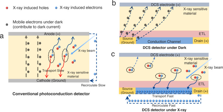
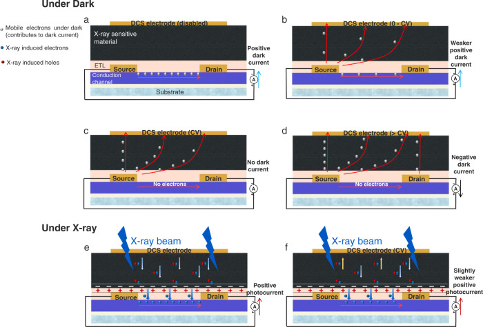
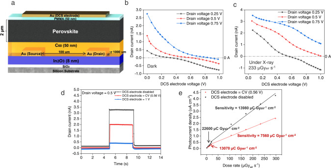
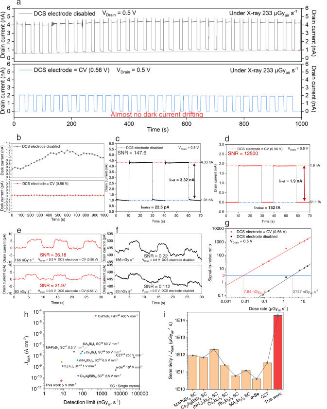
Although perovskite X-ray detectors have revealed promising properties, their dark currents are usually hundreds of times larger than the practical requirements. Here, we report a detector architecture with a unique shunting electrode working as a blanking unit to suppress dark current, and it theoretically can be reduced to zero. We experimentally fabricate the dark-current-shunting X-ray detector, which exhibits a record-low dark current of 51.1 fA at 5 V mm-1, a detection limit of 7.84 nGyair s-1, and a sensitivity of 1.3 × 10⁴ μC Gyair-1 cm-2. The signal-to-noise ratio of our polycrystalline perovskite-based detector is even outperforming many previously reported state-of-the-art single crystal-based X-ray detectors by serval orders of magnitude. Finally, the proof-of-concept X-ray imaging of a 64 × 64 pixels dark-current-shunting detector array is successfully demonstrated. This work provides a device strategy to fundamentally reduce dark current and enhance the signal-to-noise ratio of X-ray detectors and photodetectors in general.


Conflict of interest statement

The authors declare no competing interests.

Figures

Fig. 1
Fig. 1. Working mechanism of dark-current-shunting (DCS) detector and conventional photoconduction detector.
a Working mechanism of conventional photoconduction detector. The dark current and photocurrent are conducted in the same path and collected by the same electrodes. b Working mechanism of dark-current-shunting (DCS) detector. The electrons in the dark are emitted from the source and collected by the DCS electrode. c The X-ray induced electrons are generated from X-ray sensitive material and part of them drifted into a conduction channel with high carrier mobility under a built-in electric field between X-ray sensitive material and electron transport layer (ETL), then collected by drain electrode under an electric field applied in the lateral conduction channel. Even some of the X-ray induced electrons will be attracted to DCS electrode, with the high photoconductive gain effect of the conduction channel, the photocurrent is still strong.
Fig. 2
Fig. 2. Detailed working principles of dark-current-shunting (DCS) X-ray detector.
a Working principle at the dark condition and with DCS electrode disabled. The electrons emitted from the source transport through the conduction channel, and are collected by the drain, the DCS detector is working in a two-terminal mode similar as a photoconductive detector. b Working principle at the dark condition and with DCS electrode applied with a small bias. Some electrons emitted from the source are attracted by the DCS electrode, and the drain collects fewer electrons than the case described in Fig. 2a, leading to a smaller dark current. c Working principle at the dark condition and with DCS electrode applied with a CV. The electrons emitted from the source are all attracted by the DCS electrode, and the drain will not receive any electrons, leading to zero dark current in principle. d Working principle at the dark condition and with DCS electrode applied with a bias larger than CV. Some electrons are extracted from the drain and collected by the DCS electrode, leading to a negative dark current. e Working principle at X-ray illumination and with DCS electrode disabled. The DCS detector is working in a two-terminal mode similarly as the photoconduction detector. f Working principle at X-ray illumination and with DCS electrode applied with a CV. In order to minimize the dark current, the DCS electrode should be biased with a CV. Under X-ray excitation, the photo-generated excess carriers are transported through the transport layer (ETL) and sensitize the conduction channel, eventually producing photocurrent at the drain (Source electrode is always contacted to the ground, drain electrode is applied with a working voltage. Working voltage and CV here are positive).
Fig. 3
Fig. 3. Schematic, current–voltage characteristics and sensitivity of DCS X-ray detectors.
a Schematic of DCS X-ray detectors. b Current–voltage curves in terms of DCS electrode voltages and drain currents in dark conditions. The drain current decreases with increased DCS biases. c Current–voltage curves in terms of DCS electrode voltages and drain currents when exposed to X-ray. d X-ray generated pulse signals were illustrated when the DCS electrode was disabled, applied with a CV (0.56 V) and applied with a voltage larger than CV (1 V). The dose rate of X-ray was 233 μGyair s−1. e The sensitivity of the DCS detectors was calculated when the DCS electrode was disabled and applied with a CV (0.56 V).
Fig. 4
Fig. 4. Characterizations of pulse-train response, signal-to-noise ratio (SNR), and lowest detection limit.
a X-ray pulse-train response. By applying CV (0.56 V) to the DCS electrode, the signal-to-noise ratio (SNR), the pulse quality, and stability are obviously improved. There is almost no dark current drifting. b Characterization of dark current drifting. When the DCS electrode is disabled, the dark current gradually shifts from 0.615 nA to 0.986 nA. When the DCS electrode is biased with CV, the dark current reveals almost no shift during the pulse-train measurement. c The noise current and the SNR are 22.5 pA and 147.6, respectively, when the DCS electrode is disabled. d The noise current and the SNR are 0.152 pA and 12500, respectively, when DCS electrode is applied with a CV (0.56 V). e With the DCS electrode biased with a CV (0.56 V), the SNRs are 36.18 and 21.97 under respective X-ray dose rate of 166 nGyair s−1 and 83 nGyair s−1. f With the DCS electrode disabled, the SNRs are 0.22 and 0.112 under respective X-ray dose rate of 166 nGyair s−1 and 83 nGyair s−1. g Characterizations of detection limit. The detection limit (SNR = 3) of the DCS detector is as low as 7.84 nGyair s−1, which is 350 times lower than the control photoconductor detector. The lowest detection limit was estimated by the reverse extension line to where the SNR = 3. h The comparison with respect to the dark current density and the detection limit between this work and other state-of-the-art photoconduction detectors is demonstrated. The applied electric fields are noted along with the detector materials. i The sensitivity/Jdark, a figure of merit to evaluate SNR, is illustrated to compared our DCS detector and other reported state-of-the-art photoconduction detectors.
Fig. 5
Fig. 5. DCS X-ray detector array and X-ray imaging.
a Schematic illustration of the DCS X-ray detector array. b Optical image of a fraction of detector array of nine pixels. c, The pixel pitch is 312.5 μm. The photosensitive area is 30 μm × 200 μm. d Electron mobility distribution of randomly selected 400 pixels. e Stability test of the DCS detector. The X-ray photon energy is 50 keV and the dose rate is 0.85 mGyair s−1. The total received dose is 8.5 Gyair. f The image contrast is determined the value of Inet/Idark at different X-ray dose rates. g The optical image of the 64 × 64 detector array and a 2 mm thick stainless steel mask plate with a hollowed-out figure of ‘Qiushi Eagle’. h Obtained X-ray image while the DCS electrode is biased with CV (0.56 V). i Top view of the coil spring in the capsule. The coil spring cannot be seen by eyes. j Top view of the coil spring. k Obtained X-ray image of the coil spring in the capsule, with the DCS electrode biased with the CV (0.56 V).

References

    1. Zheng X, et al. Ultrasensitive and stable X-ray detection using zero-dimensional lead-free perovskites. J. Energy Chem. 2020;49:299–306.
    1. Yang B, et al. Heteroepitaxial passivation of Cs2AgBiBr6 wafers with suppressed ionic migration for X-ray imaging. Nat. Commun. 2019;10:1989. - PMC - PubMed
    1. Wei HT, Huang JS. Halide lead perovskites for ionizing radiation detection. Nat. Commun. 2019;10:12. - PMC - PubMed
    1. Wei HT, et al. Sensitive X-ray detectors made of methylammonium lead tribromide perovskite single crystals. Nat. Photon. 2016;10:333–339.
    1. Tie S, et al. Robust fabrication of hybrid lead-free perovskite pellets for stable X-ray detectors with low detection limit. Adv. Mater. 2020;32:e2001981. - PubMed