. 2023 Feb 22;23(4):1451-1458.
doi: 10.1021/acs.nanolett.2c04826. Epub 2023 Feb 7.

Core-Shell Nanorods as Ultraviolet Light-Emitting Diodes

Affiliations

Core-Shell Nanorods as Ultraviolet Light-Emitting Diodes

Douglas Cameron et al. Nano Lett. .

Abstract

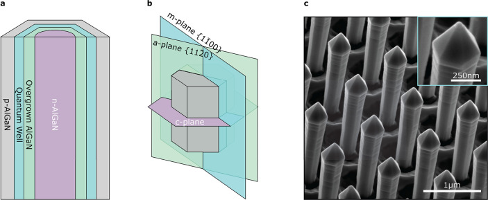
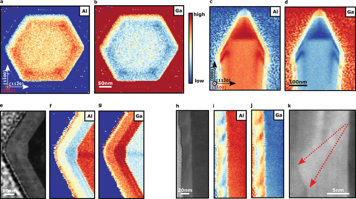
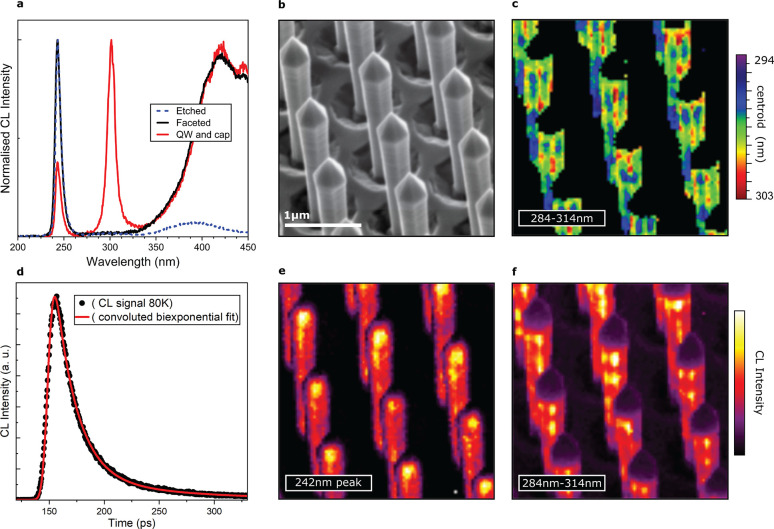
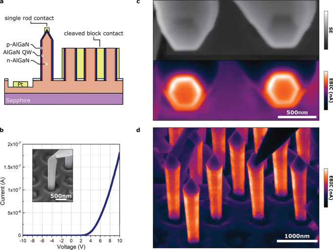
Existing barriers to efficient deep ultraviolet (UV) light-emitting diodes (LEDs) may be reduced or overcome by moving away from conventional planar growth and toward three-dimensional nanostructuring. Nanorods have the potential for enhanced doping, reduced dislocation densities, improved light extraction efficiency, and quantum wells free from the quantum-confined Stark effect. Here, we demonstrate a hybrid top-down/bottom-up approach to creating highly uniform AlGaN core-shell nanorods on sapphire repeatable on wafer scales. Our GaN-free design avoids self-absorption of the quantum well emission while preserving electrical functionality. The effective junctions formed by doping of both the n-type cores and p-type caps were studied using nanoprobing experiments, where we find low turn-on voltages, strongly rectifying behaviors and significant electron-beam-induced currents. Time-resolved cathodoluminescence measurements find short carrier liftetimes consistent with reduced polarization fields. Our results show nanostructuring to be a promising route to deep-UV-emitting LEDs, achievable using commercially compatible methods.

Keywords: AlGaN; UV LED; core−shell; electron microscopy; nanowire; semiconductor.


Conflict of interest statement

The authors declare no competing financial interest.

Figures

Figure 1
Figure 1
Nanorod core–shell architecture. (a) Schematic of core–shell structures employed in this work (not to scale), with n-AlGaN cores, quantum wells, and p-AlGaN shells forming a full LED structure. (b) Frequently discussed crystal planes relating to our rods, which also identify the orientation of our TEM lamellae. (c) SE image of the nanorod array with clear uniformity in pitch and rod dimensions. Scale bar is 1 μm. A higher magnification inset (with a 250 nm scale bar) shows a spherical feature at the tip of a rod.
Figure 2
Figure 2
TEM–EDS elemental composition maps. (a) Low-magnification map of the first section looking along the c direction. The Al X-ray peak intensity variation within the core reveals increased Al incorporation on the a axes. (b) Ga K- and L-line X-ray peak intensities within the core showing the inverse of the Al map as expected. (c and d) Low-magnification map of the second section looking through the m direction. The formation of the “broadhead” can be seen here. (e) Higher magnification high-angle annular dark-field (HAADF) image focusing at one of the corners of the hexagonal structure. Z contrast in the images reveals the location of the core, quantum well, and p-AlGaN capping layer. The formation of a distinct a plane at the edge of the core is clear. (f) Al X-ray peak intensity showing both the increased Al incorporation when moving from the core center along the a direction and decreased Al in the quantum well on the a-plane facet. (g) Ga X-ray peak intensity with the core again showing the inverse of the Al map as expected. (h, i, and j) HAADF and Al and Ga X-ray peak intensities over the same area, showing alloy fluctuations along the quantum well. The Ga-rich composition develops in a semipolar direction from the a plane. (k) Higher magnification HAADF TEM image focusing along one of the a planes. Here, we can see the exacerbation of surface roughness as growth progresses outward.
Figure 3
Figure 3
Results from room-temperature, low-temperature, and time-resolved CL hyperspectral studies. (a) CL spectra from the three samples at room temperature: the etched cores, the etched cores following refaceting, and the etched cores following QW and cap growth. Each spectrum was taken by averaging a number of pixels from maps of each sample (taking care to avoid regions where the “substrate” was scanned directly) and was then normalized to a maximum. (b) Secondary electron (SE) image of the area mapped. (c) Map showing the shift in energy of the quantum well emission, with red shifts at the m-plane intersections (a plane). The noise-dominated substrate region has been masked in this map for clarity. (d) Fitted decay of the m-plane quantum well emission accounting for the instrument response function. (e) Map showing the uniform band edge emission peak intensity from the core. (f) CL intensity of the quantum well emission showing distinct high-intensity clusters at the a plane along with lower emission intensity from the rest of the m-plane sidewalls. Emission from the top semipolar facets is notably absent.
Figure 4
Figure 4
Electrical characterization of our core–shell LED structures. (a) Schematic of our nanorod electrical testing architecture. Using FIB–SEM, a common n contact was created by milling down into the n layer and a Pt pad and then deposited. The p contacts were produced in two forms: Pt was either carefully deposited on the apex of single rods or infilled around many rods to create blocks, which had been cleaved (again using the FIB), to reveal previously obscured inner junctions. (b) Example IV curve for a single rod contacted with a nanoprobe as seen in the featured inset. This shows strong rectification, indicating the successful formation of a p–n junction. (c) SE (grayscale) and EBIC images of the cleaved block contact viewed from above, showing the presence of the junction around the entire circumference of the rods as intended. (d) EBIC image of a single-rod contact, with the nanoprobe contacting from above.

References

    1. Amano H.; Collazo R.; De Santi C.; Einfeldt S.; Funato M.; Glaab J.; Hagedorn S.; Hirano A.; Hirayama H.; Ishii R.; Kashima Y.; Kawakami Y.; Kirste R.; Kneissl M.; Martin R.; Mehnke F.; Meneghini M.; Ougazzaden A.; Parbrook P. J; Rajan S.; Reddy P.; Romer F.; Ruschel J.; Sarkar B.; Scholz F.; Schowalter L. J; Shields P.; Sitar Z.; Sulmoni L.; Wang T.; Wernicke T.; Weyers M.; Witzigmann B.; Wu Y.-R.; Wunderer T.; Zhang Y. The 2020 UV emitter roadmap. J. Phys. D: Appl. Phys. 2020, 53, 503001.10.1088/1361-6463/aba64c. - DOI
    1. Kneissl M.; Seong T.-Y.; Han J.; Amano H. The emergence and prospects of deep-ultraviolet light-emitting diode technologies. Nat. Photonics 2019, 13, 233.10.1038/s41566-019-0359-9. - DOI
    1. Würtele M.; Kolbe T.; Lipsz M.; Külberg A.; Weyers M.; Kneissl M.; Jekel M. Application of GaN-based ultraviolet-C light emitting diodes–UV LEDs–for water disinfection. Water Res. 2011, 45, 1481.10.1016/j.watres.2010.11.015. - DOI - PubMed
    1. Inagaki H.; Saito A.; Sugiyama H.; Okabayashi T.; Fujimoto S. Rapid inactivation of SARS-CoV-2 with deep-UV LED irradiation. Emerging Microbes Infect. 2020, 9, 1744.10.1080/22221751.2020.1796529. - DOI - PMC - PubMed
    1. Glaab J.; Lobo-Ploch N.; Cho H. K.; Filler T.; Gundlach H.; Guttmann M.; Hagedorn S.; Lohan S. B.; Mehnke F.; Schleusener J.; Sicher C.; Sulmoni L.; Wernicke T.; Wittenbecher L.; Woggon U.; Zwicker P.; Kramer A.; Meinke M. C.; Kneissl M.; Weyers M.; Winterwerber U.; Einfeldt S. Skin tolerant inactivation of multiresistant pathogens using far-UVC LEDs. Sci. Rep. 2021, 11, 1.10.1038/s41598-021-94070-2. - DOI - PMC - PubMed