. 2022 Dec 6;5(3):675-684.
doi: 10.1039/d2na00552b. eCollection 2023 Jan 31.

Integration of photovoltaic and photogating effects in a WSe2/WS2/p-Si dual junction photodetector featuring high-sensitivity and fast-response

Affiliations

Integration of photovoltaic and photogating effects in a WSe2/WS2/p-Si dual junction photodetector featuring high-sensitivity and fast-response

Zihao Huang et al. Nanoscale Adv. .

Abstract

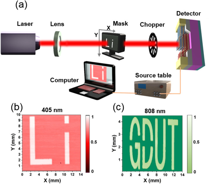
Two-dimensional (2D) material-based van der Waals (vdW) heterostructures with exotic semiconducting properties have shown tremendous potential in next-generation photovoltaic photodetectors. Nevertheless, these vdW heterostructure devices inevitably suffer from a compromise between high sensitivity and fast response. Herein, an ingenious photovoltaic photodetector based on a WSe2/WS2/p-Si dual-vdW heterojunction is demonstrated. First-principles calculations and energy band profiles consolidate that the photogating effect originating from the bottom vdW heterojunction not only strengthens the photovoltaic effect of the top vdW heterojunction, but also suppresses the recombination of photogenerated carriers. As a consequence, the separation of photogenerated carriers is facilitated and their lifetimes are extended, resulting in higher photoconductive gain. Coupled with these synergistic effects, this WSe2/WS2/p-Si device exhibits both high sensitivity (responsivity of 340 mA W-1, a light on/off ratio greater than 2500, and a detectivity of 3.34 × 10¹¹ Jones) and fast response time (rise/decay time of 657/671 μs) under 405 nm light illumination in self-powered mode. Finally, high-resolution visible-light and near-infrared imaging capabilities are demonstrated by adopting this dual-heterojunction device as a single pixel, indicating its great application prospects in future optoelectronic systems.


Conflict of interest statement

The authors declare no competing financial interests.

Figures

Fig. 1
Fig. 1. Schematic drawing of the fabrication procedure of the HDH device.
Fig. 2
Fig. 2. Structural properties of the HDH photodetector. (a) Optical micrograph of the HDH device. The WSe2 and WS2 flakes are highlighted in blue and red dotted lines, respectively. (b and c) HRTEM images of WS2 and WSe2 and the insets show the corresponding FFT patterns, respectively. (d) AFM image measured at the green solid line in (a). The inset shows the height profile across the white line in (d). The thicknesses of WS2 and WSe2 are 76.4 nm and 79.1 nm, respectively. KPFM images obtained from the interfaces of (e) WS2/p-Si and (f) WSe2/WS2. The inset shows the potential profiles across the corresponding white lines. The potential difference between WS2 and p-Si is 109.1 mV, and the potential difference between WSe2 and WS2 is 25.6 mV.
Fig. 3
Fig. 3. Optoelectronic characteristics of the HDH photodetector. (a) Electrical connections of the device. (b) PL spectra collected from WSe2, WS2, and HDH. (c) Spectral photoresponse of the device under the illumination of 400–1100 nm light. (d) IV curves in the dark and under 405 nm light (102.69 mW cm−2). The maximum light on/off ratio exceeds 40 000. (e) Comparison of the light on/off ratio of the devices with different architectures at a bias of 0 V. (f) Plots of electrical power under different intensities of 405 nm light.
Fig. 4
Fig. 4. Photodetection metrics of the HDH device in self-powered mode. Calculated (a) photocurrent, (b) responsivity, (c) detectivity, and (d) photoconductive gain of the HDH and WSe2–WS2 devices as functions of incident power density at a bias of 0 V. (e) Comparison of R and D* of the HDH device against those of other reported self-driven devices at 0 V bias, including Cs2AgBiBr6, graphene/GaAs, WS2/Si, graphene/InSe/MoS2, ZnO MW/PEDOT:PSS, ZnO:Ga MW/PEDOT:PSS, CsBi3I10 perovskite/Si, (FAPbI3)0.97(MAPbBr3)0.03, MoSe2/FePS3, and Si NW array/Cs-doped FAPbI3. (f) Response time of the HDH device at a bias voltage of 0 V.
Fig. 5
Fig. 5. Working mechanism of the HDH photodetector. Band decomposed charge density in the WSe2/WS2/p-Si dual heterojunctions for (a) CBM and (b) VBM. (c) Charge density difference in the WSe2/WS2/p-Si dual heterojunctions. The yellow and cyan areas indicate electron accumulation and depletion, respectively. (d) Plane-averaged charge density difference along the z direction (black line in panel c). Positive and negative values represent electron accumulation and depletion, respectively. (e) Schematic diagram of the energy band structures of WSe2/WS2/p-Si before contact. (f) Band alignments and charge transfer of the dual junction device under illumination. (g) Cross-sectional diagram of the HDH device. The electrodes extract photoexcited carriers and generate photocurrent. Photoexcited holes accumulated in p-Si will generate the Egating.
Fig. 6
Fig. 6. Imaging application of the HDH device. (a) Schematic diagram of the measurement system for visible-NIR single-pixel imaging applications. (b) The resulting image of “Li” under 405 nm light illumination. (c) The resulting image of “GDUT” under 808 nm light illumination.

References

    1. Long M. Wang P. Fang H. Hu W. Progress, Challenges, and Opportunities for 2D Material Based Photodetectors. Adv. Funct. Mater. 2018;29(19):1803807. doi: 10.1002/adfm.201803807. - DOI
    1. Cui X. Lee G.-H. Kim Y. D. Arefe G. Huang P. Y. Lee C.-H. Chenet D. A. Zhang X. Wang L. Ye F. Pizzocchero F. Jessen B. S. Watanabe K. Taniguchi T. Muller D. A. Low T. Kim P. Hone J. Multi-terminal transport measurements of MoS2 using a van der Waals heterostructure device platform. Nat. Nanotechnol. 2015;10(6):534–540. doi: 10.1038/nnano.2015.70. - DOI - PubMed
    1. Huo N. Konstantatos G. Recent Progress and Future Prospects of 2D-Based Photodetectors. Adv. Mater. 2018;30(51):1801164. doi: 10.1002/adma.201801164. - DOI - PubMed
    1. Zhou Y. Nie Y. Liu Y. Yan K. Hong J. Jin C. Zhou Y. Yin J. Liu Z. Peng H. Epitaxy and Photoresponse of Two-dimensional GaSe Crystals on Flexible Transparent Mica Sheets. ACS Nano. 2014;8(2):1485–1490. doi: 10.1021/nn405529r. - DOI - PubMed
    1. Chen Y. Wang Y. Wang Z. Gu Y. Ye Y. Chai X. Ye J. Chen Y. Xie R. Zhou Y. Hu Z. Li Q. Zhang L. Wang F. Wang P. Miao J. Wang J. Chen X. Lu W. Zhou P. Hu W. Unipolar barrier photodetectors based on van der Waals heterostructures. Nat. Electron. 2021;4(5):357–363. doi: 10.1038/s41928-021-00586-w. - DOI