

Recent Developments of High-Pressure Spark Plasma Sintering: An Overview of Current Applications, Challenges and Future Directions
- PMID: 36770003
- PMCID: PMC9919817
- DOI: 10.3390/ma16030997
Recent Developments of High-Pressure Spark Plasma Sintering: An Overview of Current Applications, Challenges and Future Directions
Abstract
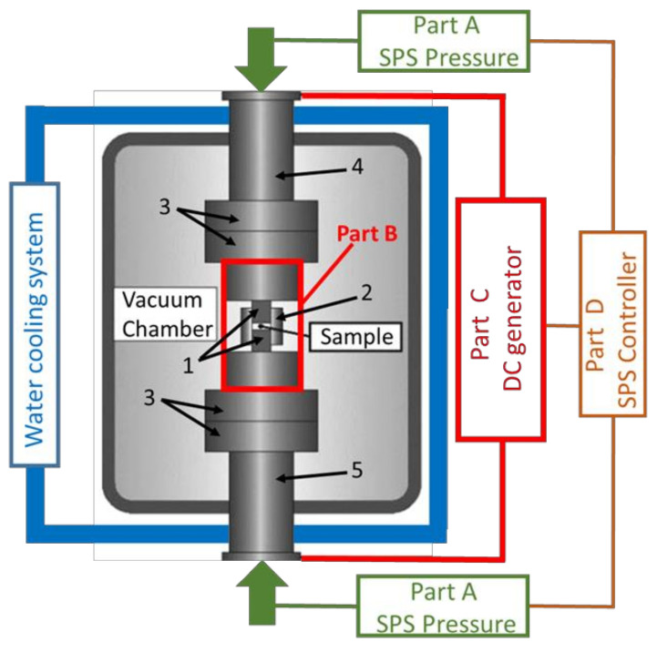
Spark plasma sintering (SPS), also called pulsed electric current sintering (PECS) or field-assisted sintering technique (FAST) is a technique for sintering powder under moderate uniaxial pressure (max. 0.15 GPa) and high temperature (up to 2500 °C). It has been widely used over the last few years as it can achieve full densification of ceramic or metal powders with lower sintering temperature and shorter processing time compared to conventional processes, opening up new possibilities for nanomaterials densification. More recently, new frontiers of opportunities are emerging by coupling SPS with high pressure (up to ~10 GPa). A vast exciting field of academic research is now using high-pressure SPS (HP-SPS) in order to play with various parameters of sintering, like grain growth, structural stability and chemical reactivity, allowing the full densification of metastable or hard-to-sinter materials. This review summarizes the various benefits of HP-SPS for the sintering of many classes of advanced functional materials. It presents the latest research findings on various HP-SPS technologies with particular emphasis on their associated metrologies and their main outstanding results obtained. Finally, in the last section, this review lists some perspectives regarding the current challenges and future directions in which the HP-SPS field may have great breakthroughs in the coming years.
Keywords: HP-SPS; high pressure; spark plasma sintering.
Conflict of interest statement
The authors declare no conflict of interest.
Figures


Similar articles
-
High Pressure (HP) in Spark Plasma Sintering (SPS) Processes: Application to the Polycrystalline Diamond.Materials (Basel). 2022 Jul 9;15(14):4804. doi: 10.3390/ma15144804. Materials (Basel). 2022. PMID: 35888270 Free PMC article.
-
Zirconium Carbide Produced by Spark Plasma Sintering and Hot Pressing: Densification Kinetics, Grain Growth, and Thermal Properties.Materials (Basel). 2016 Jul 14;9(7):577. doi: 10.3390/ma9070577. Materials (Basel). 2016. PMID: 28773697 Free PMC article.
-
High-Pressure Spark Plasma Sintering (HP SPS): A Promising and Reliable Method for Preparing Ti-Al-Si Alloys.Materials (Basel). 2017 Apr 27;10(5):465. doi: 10.3390/ma10050465. Materials (Basel). 2017. PMID: 28772824 Free PMC article.
-
Fabrication of Porous Materials by Spark Plasma Sintering: A Review.Materials (Basel). 2019 Feb 12;12(3):541. doi: 10.3390/ma12030541. Materials (Basel). 2019. PMID: 30759751 Free PMC article. Review.
-
Comparison of Reactive and Non-Reactive Spark Plasma Sintering Routes for the Fabrication of Monolithic and Composite Ultra High Temperature Ceramics (UHTC) Materials.Materials (Basel). 2013 Apr 29;6(5):1566-1583. doi: 10.3390/ma6051566. Materials (Basel). 2013. PMID: 28809229 Free PMC article. Review.
Cited by
-
Testing for Abrasion Resistance of WC-Co Composites for Blades Used in Wood-Based Material Processing.Materials (Basel). 2023 Aug 25;16(17):5836. doi: 10.3390/ma16175836. Materials (Basel). 2023. PMID: 37687529 Free PMC article.
-
Development of an Alternative Manufacturing Technology for Niobium Components.Materials (Basel). 2024 Jun 24;17(13):3093. doi: 10.3390/ma17133093. Materials (Basel). 2024. PMID: 38998176 Free PMC article.
-
Radiation Synthesis of High-Temperature Wide-Bandgap Ceramics.Micromachines (Basel). 2023 Nov 30;14(12):2193. doi: 10.3390/mi14122193. Micromachines (Basel). 2023. PMID: 38138362 Free PMC article. Review.
-
The Optimization of Radiation Synthesis Modes for YAG:Ce Ceramics.Materials (Basel). 2023 Apr 17;16(8):3158. doi: 10.3390/ma16083158. Materials (Basel). 2023. PMID: 37109993 Free PMC article.
-
C.P titanium/Ti-6Al-4V joint by spark plasma welding: Microstructure and mechanical properties.Heliyon. 2024 Mar 3;10(6):e27514. doi: 10.1016/j.heliyon.2024.e27514. eCollection 2024 Mar 30. Heliyon. 2024. PMID: 38509952 Free PMC article.
References
-
- Suárez M., Fernández A., Menéndez J., Torrecillas R., Kessel H., Hennicke J., Kirchner R., Kessel T. Challenges and opportunities for spark plasma sintering: A key technology for a new generation of materials. Sinter. Appl. 2013;13:319–342.
-
- Zhang Z.-H., Liu Z.-F., Lu J.-F., Shen X.-B., Wang F.-C., Wang Y.-D. The sintering mechanism in spark plasma sintering–proof of the occurrence of spark discharge. Scr. Mater. 2014;81:56–59. doi: 10.1016/j.scriptamat.2014.03.011. - DOI
-
- Sakka Y., Grasso S. Pulsed electrodischarged pressure sintering and flash sintering, a review. Mater. Today Proc. 2019;16:14–24. doi: 10.1016/j.matpr.2019.05.288. - DOI
-
- Chaim R., Chevallier G., Weibel A., Estournès C. Grain growth during spark plasma and flash sintering of ceramic nanoparticles: A review. J. Mater. Sci. 2018;53:3087–3105. doi: 10.1007/s10853-017-1761-7. - DOI
Publication types
LinkOut - more resources
Full Text Sources
Research Materials
Miscellaneous
