. 2023 Feb 11;13(1):2451.
doi: 10.1038/s41598-023-29128-4.

In-situ atomic level observation of the strain response of graphene lattice

Affiliations

In-situ atomic level observation of the strain response of graphene lattice

Jz-Yuan Juo et al. Sci Rep. .

Abstract

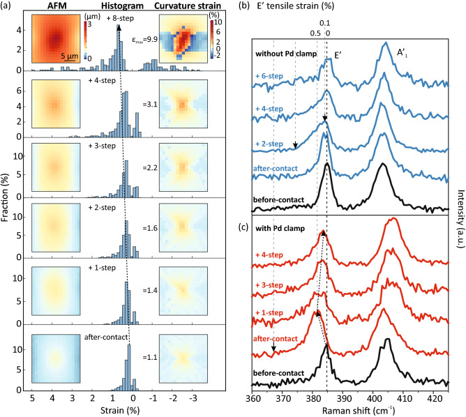
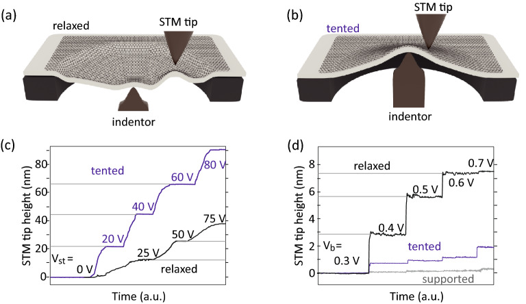
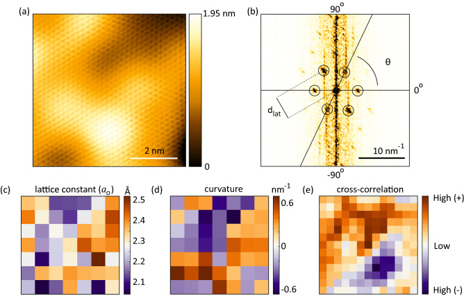
Strain is inevitable in two-dimensional (2D) materials, regardless of whether the film is suspended or supported. However, the direct measurement of strain response at the atomic scale is challenging due to the difficulties of maintaining both flexibility and mechanical stability at low temperature under UHV conditions. In this work, we have implemented a compact nanoindentation system with a size of [Formula: see text] 160 mm[Formula: see text] [Formula: see text] 5.2 mm in a scanning tunneling microscope (STM) sample holder, which enables the reversible control of strain and gate electric field. A combination of gearbox and piezoelectric actuator allowed us to modulate the depth of the indentation continuously with nanometer precision. The 2D materials were transferred onto the polyimide film. Pd clamp was used to enhance the strain transfer from the polyimide from to the 2D layers. Using this unique technique, strain response of graphene lattice were observed at atomic precision. In the relaxed graphene, strain is induced mainly by local curvature. However, in the strained graphene with tented structure, the lattice parameters become more sensitive to the indentor height change and stretching strain is increased additionally. Moreover, the gate controllability is confirmed by measuring the dependence of the STM tip height on gate voltage.


Conflict of interest statement

The authors declare no competing interests.

Figures

Figure 1
Figure 1
The schematic of strain- and gate-controllable STM structure. Vb and Vg are bias and gate voltages applied on the sample, respectively.
Figure 2
Figure 2
Design of strain- and gate-controllable STM sample holder. (a) 3D model top view. (b) Cross section of A-B line drawn in (a). (c) Detailed side view of the strained junction. (d) Top view of the sample area. (e) Optical images of STM tunneling junction where the strain conditions of sample are controlled using gearbox system. (f) Photograph of the sample holder.
Figure 3
Figure 3
Height controllability of the sample and the indentor using gearbox and piezoelectric actuator (a) AFM topography images of polyimide surfaces taken before and after moving the polyimide film down by 8-steps using the gearbox. A step is defined as the height change when one tooth of a side gear is moved. (b) Height changes by gearbox control. Line profiles are taken from the center of the deformed area, shown as the black dotted line in (a). Δh is the height difference between the highest and lowest points in the image. The position with the maximum height is defined as the center point (x= 0). (c) Height changes by piezoelectric control. The piezoelectric actuator moves around 1.8 μm under an applied voltage (Vst) of 100 V at room temperature.
Figure 4
Figure 4
Characterization of strain distribution. (a) Calculation of the curvature-induced strain distribution based on the AFM topography images measured on the polyimide film before transferring the 2D material that were shown in Fig. 3. (b, c) Raman spectra taken at the indented center of monolayer MoS2 transferred on polyimide film with increasing the number of gear steps. (b) is with and (c) is without a Pd clamp.
Figure 5
Figure 5
STM measurement on the graphene transferred on polyimide film. (a) Strain-free (relaxed) condition and (b) tented distortion induced by strain applied using the gearbox based control system. The sample height dependence on the piezoelectric actuator voltage (Vst), and the sample bias voltage (Vb) are shown in (c) and (d), respectively.
Figure 6
Figure 6
(a) Atomic-resolution image of graphene in the relaxed case and (b) its fast-Fourier transformation converted image with six clear lattice points. (ce) The map of local average graphene lattice constant (a0) and local curvature calculated from (a) and their cross-correlation.
Figure 7
Figure 7
Characterization of strain-controllability. The boxplots of local graphene lattice points in (a) relaxed and (b) tented cases with increasing piezoelectric actuator voltage (Vst). For each lattice point, dlat is the length of reciprocal lattice vector, and θ is the angle defined by comparing with the horizon, 0-line drawn in (c). (c) The schematic summarises how graphene is deformed in the tented case when increasing Vst, based on the shifts in the medians extracted from (b). The changes in the schematic are exaggerated for clarity.

References

    1. Meyer JC, et al. The structure of suspended graphene sheets. Nature. 2007;446:60–63. doi: 10.1038/nature05545. - DOI - PubMed
    1. Lee C, Wei XD, Kysar JW, Hone J. Measurement of the elastic properties and intrinsic strength of monolayer graphene. Science. 2008;321:385–388. doi: 10.1126/science.1157996. - DOI - PubMed
    1. Dai ZH, Liu LQ, Zhang Z. Strain engineering of 2d materials: Issues and opportunities at the interface. Adv. Mater. 2019 doi: 10.1002/adma.201805417. - DOI - PubMed
    1. Shin BG, et al. Indirect bandgap puddles in monolayer mos2 by substrate-induced local strain. Adv. Mater. 2016 doi: 10.1002/adma.201602626. - DOI - PubMed
    1. Rhodes D, Chae SH, Ribeiro-Palau R, Hone J. Disorder in van der waals heterostructures of 2d materials. Nat. Mater. 2019;18:541–549. doi: 10.1038/s41563-019-0366-8. - DOI - PubMed