. 2023 Feb 18;13(1):2881.
doi: 10.1038/s41598-023-30160-7.

Phase-change materials based on amorphous equichalcogenides

Affiliations

Phase-change materials based on amorphous equichalcogenides

Roman Golovchak et al. Sci Rep. .

Abstract

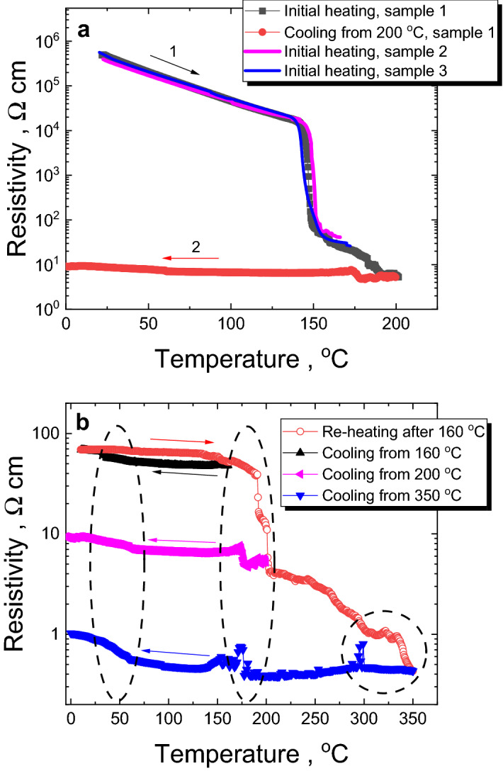
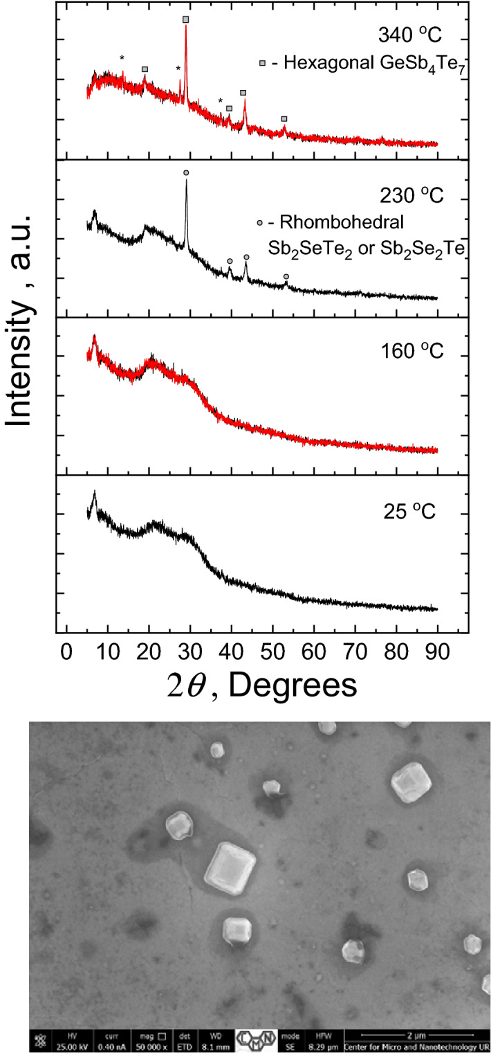
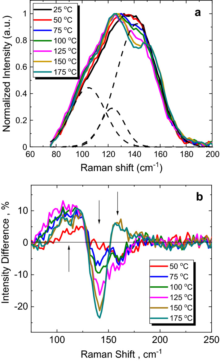
Phase-change materials, demonstrating a rapid switching between two distinct states with a sharp contrast in electrical, optical or magnetic properties, are vital for modern photonic and electronic devices. To date, this effect is observed in chalcogenide compounds based on Se, Te or both, and most recently in stoichiometric Sb2S3 composition. Yet, to achieve best integrability into modern photonics and electronics, the mixed S/Se/Te phase change medium is needed, which would allow a wide tuning range for such important physical properties as vitreous phase stability, radiation and photo-sensitivity, optical gap, electrical and thermal conductivity, non-linear optical effects, as well as the possibility of structural modification at nanoscale. In this work, a thermally-induced high-to-low resistivity switching below 200 °C is demonstrated in Sb-rich equichalcogenides (containing S, Se and Te in equal proportions). The nanoscale mechanism is associated with interchange between tetrahedral and octahedral coordination of Ge and Sb atoms, substitution of Te in the nearest Ge environment by S or Se, and Sb-Ge/Sb bonds formation upon further annealing. The material can be integrated into chalcogenide-based multifunctional platforms, neuromorphic computational systems, photonic devices and sensors.


Conflict of interest statement

The authors declare no competing interests.

Figures

Figure 1
Figure 1
As-prepared Ge15Sb40S15Se15Te15 bulk glass. Main figure shows featureless XRD pattern verifying vitreous nature of the obtained bulk material. The insert shows an ingot as removed from the ampoule and its IR image, testifying good homogeneity of the prepared bulk glass.
Figure 2
Figure 2
FTIR spectra of as-prepared Ge15Sb40S15Se15Te15 glass. The glass is transparent within 2–12 μm wavelengths range. The insert shows transmission in the fundamental optical absorption edge region.
Figure 3
Figure 3
DSC curves of as-prepared bulk Ge15Sb40S15Se15Te15 glass and thin film. (a) DSC signals for the bulk samples were recorded with 2 (black), 5 (red), 10 (blue), 15 (magenta) and 20 (orange) K/min heating rates. They show glass transition range (insert) and exothermal crystallization peaks above 300 °C. (b) DSC curves of thin Ge15Sb40S15Se15Te15 films scraped out of glass substrate show low-temperature shift of main crystallization peak and additional crystallization peaks within ~ 160–200 °C range.
Figure 4
Figure 4
Thermodynamic parameters calculated from DSC data. (a) Ozawa’s and Kissinger’s plots for activation energy calculations. (b) Probe z(α) curves, calculated from DSC data of the as-prepared bulk Ge15Sb40S15Se15Te15 glass, showing peak values shifted from 0.63 position required for JMA model to be valid.
Figure 5
Figure 5
(a) The SEM image of the cross-section of amorphous Ge15Sb40S15Se15Te15 thin film as-deposited on microscopy slide wafer, showing uniform thickness and absence of large-scale inhomogeneities and pores. (b) SEM elemental imaging across the cross-section of the film (on the very left), testifying more or less uniform distribution of chemical elements throughout the entire film thickness.
Figure 6
Figure 6
(a) Temperature dependence of resistivity measured in heating (step 1) and cooling (step 2) modes with 5 K/min rate for a fresh Ge15Sb40S15Se15Te15 thin film, deposited on high-density Al2O3 ceramic substrate with interdigitated electrodes (sample 1), shows rapid switching between High- and Low-resistivity states at ~ 145 °C. To demostrate the influence of small (within 3 at.%) variation in composition on the phase change effect, the temperature dependences of resistivity in heating mode (5 K/min) are shown for the samples 2 and 3 obtained in different synthesis using similar technique and parameters. (b) If the previously heated to 160 °C sample is cooled (black) and re-heated again (red) up to 350 °C, a number of features can be observed on resistivity vs temperature dependences upon heating and cooling (circled regions).
Figure 7
Figure 7
In situ XRD studies at different temperatures. The patterns of Ge15Sb40S15Se15Te15 thin film deposited on microscopy slide, recorded at different target temperatures (each achieved with heating ramp of 5 K/min), are featureless until ~ 175 °C. Bottom panel shows SEM image of crystallites formed on the surface of the film after annealing at 340 °C.
Figure 8
Figure 8
(a) Unpolarized Raman spectra of amorphous Ge15Sb40S15Se15Te15 thin film recorded at different temperatures show typical pattern of Te-based complexes (they are dominated in Raman signal of the investigated glasses). The example of unrestricted Gaussian fit (dashed lines) performed for the signal at 25 °C shows features common to other GST materials. (b) Difference between the Raman spectra at indicated temperatures and the 25 °C temperature one gives important information on the temperature-induced transformations in studied material.
Figure 9
Figure 9
XPS results (bold line—experimental curve; thin lines—fitting components). Comparison of the XPS spectra, recorded for Ge15Sb40S15Se15Te15 thin film in as-prepared amorphous and annealed at 175 °C states, shows significant difference for Sb, Ge and S core levels. This allows to further refine the mechanism proposed on the basis of Raman and XRD studies.

References

    1. Kim T. Evolution of phase-change memory for the storage-class memory and beyond. IEEE Trans. Electron Devices. 2020;67:1394–1406. doi: 10.1109/TED.2020.2964640. - DOI
    1. Fantini P. Phase change memory applications: The history, the present and the future. J. Phys. D Appl. Phys. 2020;53:283002. doi: 10.1088/1361-6463/ab83ba. - DOI
    1. Wuttig M, Yamada N. Phase-change materials for rewritable data storage. Nat. Mater. 2007;6:824–832. doi: 10.1038/nmat2009. - DOI - PubMed
    1. Zhang Y, Chou JB, Li J, Li H, Du Q, Yadav A, Zhou S, Shalaginov MY, Fang Zh, Zhong H, Roberts Ch, Robinson P, Bohlin B, Ríos C, Lin H, Kang M, Gu T, Warner J, Liberman V, Richardson K, Hu J. Broadband transparent optical phase change materials for high-performance nonvolatile photonics. Nat. Comm. 2019;10:4279. doi: 10.1038/s41467-019-12196-4. - DOI - PMC - PubMed
    1. Xu P, Zheng J, Doylend JK, Majumdar A. Low-loss and broadband nonvolatile phase-change directional coupler switches. ACS Photon. 2019;6:553–557. doi: 10.1021/acsphotonics.8b01628. - DOI