. 2023 Feb 20;14(1):932.
doi: 10.1038/s41467-023-36141-8.

Open-circuit and short-circuit loss management in wide-gap perovskite p-i-n solar cells

Affiliations

Open-circuit and short-circuit loss management in wide-gap perovskite p-i-n solar cells

Pietro Caprioglio et al. Nat Commun. .

Abstract

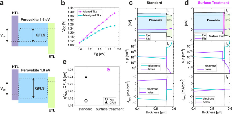
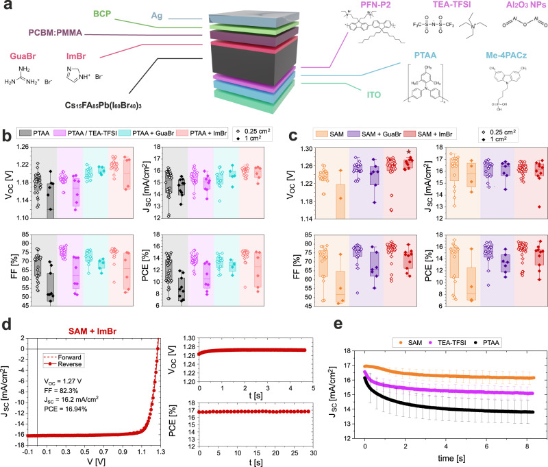
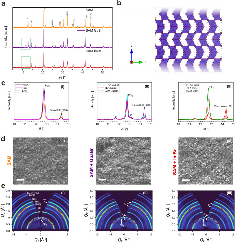
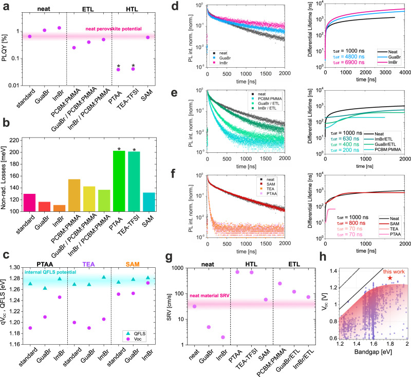
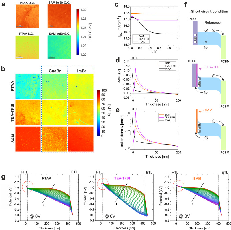
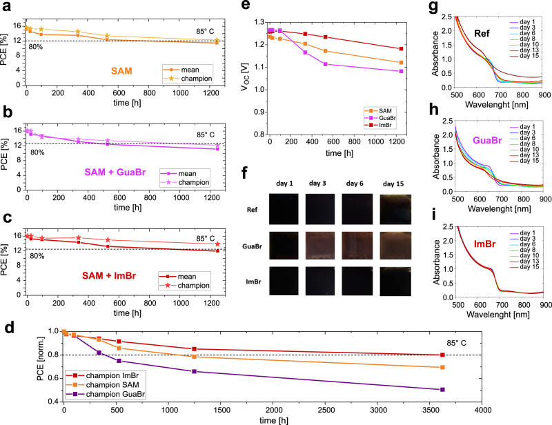
In this work, we couple theoretical and experimental approaches to understand and reduce the losses of wide bandgap Br-rich perovskite pin devices at open-circuit voltage (VOC) and short-circuit current (JSC) conditions. A mismatch between the internal quasi-Fermi level splitting (QFLS) and the external VOC is detrimental for these devices. We demonstrate that modifying the perovskite top-surface with guanidinium-Br and imidazolium-Br forms a low-dimensional perovskite phase at the n-interface, suppressing the QFLS-VOC mismatch, and boosting the VOC. Concurrently, the use of an ionic interlayer or a self-assembled monolayer at the p-interface reduces the inferred field screening induced by mobile ions at JSC, promoting charge extraction and raising the JSC. The combination of the n- and p-type optimizations allows us to approach the thermodynamic potential of the perovskite absorber layer, resulting in 1 cm2 devices with performance parameters of VOCs up to 1.29 V, fill factors above 80% and JSCs up to 17 mA/cm2, in addition to a thermal stability T80 lifetime of more than 3500 h at 85 °C.


Conflict of interest statement

H.J.S. is the founder and Chief Scientific Officer of Oxford Photovoltaics, a company commercialising perovskite photovoltaics. The remaining authors declare no competing interests.

Figures

Fig. 1
Fig. 1. Drift-diffusion simulations.
a Schematic diagram representing 1.6 eV and 1.8 eV perovskite solar cells using a hole and electron transport layer optimized for the 1.6 eV cell. The relation between the internal QFLS and external VOC is indicated by the dotted lines. b VOC obtained from drift-diffusion simulations for a perovskite solar cell device with varying energy gap. The purple data points represent a case where the energy levels of the transport layers are adjusted according to the perovskite bandgap in order maintain ideal alignment, whereas the turquoise points illustrate the effect of the energy levels remaining the same as those optimized for the 1.6 eV device. c Band structure and quasi-Fermi levels (Fe and Fh) at VOC conditions close to the ETL side obtained from a drift-diffusion simulation of a standard 1.8 eV perovskite device. The respective hole and electron densities and the total hole and electron recombination currents (Jrec.) are also reported. d Band structure and quasi-Fermi levels at VOC conditions as in c for a 1.8 eV device implementing a modified perovskite where the surface at the ETL side features a lower valence band and wider bandgap. e QFLS and VOC relation from the devices simulated in ce.
Fig. 2
Fig. 2. Device characterization.
a Illustration of the typical 1.8 eV perovskite pin device used in this work. All the possible device architecture variations investigated in this study are also represented with their respective chemical structures. b Device statistic of a series of interface optimizations on perovskite devices using PTAA as the HTL obtained from reverse JV scans with a scan rate of 0.3 V/s. Here a PCE cut off was applied for devices with PCEs less than half of the mean value. c Performance metrics for surface-treated perovskite devices using Me-4PACz as the HTL, obtained from reverse JV scans with a scan rate of 0.3 V/s. Here a PCE cut off was applied for devices with PCE lower than half of the mean value. The star indicates the record steady-state VOC for the 1 cm2 device presented in Fig. S9. d Forward and reverse JV scans of the champion device using Me-4PACz as HTL, PCBM as ETL and ImBr as perovskite surface treatment. The JV parameters are reported for the reverse scans. The steady-state PCE under maximum power point (MPP) conditions is reported for 30 s. e Steady-state JSC decays over time averaged over 10–15 devices for each HTL. The measurement is taken by holding the device at VOC conditions and switching to JSC immediately afterwards. Error bars indicate the standard deviation.
Fig. 3
Fig. 3. Structural and morphological characterization.
a XRD patterns for neat SAM/perovskite films and after treatment with GuaBr or ImBr. Additional experimental details in SI. Indices are for the cubic perovskite phase, and secondary phases are marked: PbI2 with *, ITO with #, GuaBr-induced phase with ‘G’ and ImBr-induced phase with ‘I’. b Illustration of a mixed-halide 4H polytype, identified following the surface treatments (structure modified from reference Gratia et al.). c Highlighted regions comparing XRD for all (i) neat, (ii) GuaBr-treated and (iii) ImBr-treated films, full XRD patterns for TEA-TFSI and PTAA samples is given in Figs. S17–18. d Scanning electron microscopy images of the perovskite surfaces in partially completed devices using (i) Me-4PACz and after treatment with (ii) GuaBr and (iii) ImBr (further SEM for all samples in Fig. S23), with scale bar = 1 μm. e 2D GIWAXS patterns for (i) SAM, f (ii) SAM GuaBr and (iii) SAM ImBr films, collected with a grazing incidence angle of 1°. 1D integrations of the data are given in Fig. S23.
Fig. 4
Fig. 4. Charge recombination and energy losses.
a PLQY results for different perovskite films and half-stacks (with either an ETL or HTL) illuminated with a 532 nm laser at a 1 sun equivalent intensity. The luminescence potential range of the neat perovskite on glass is highlighted in translucent pink. b Non-radiative recombination losses with respect to the radiative thermodynamic limit of the perovskite absorber calculated from the PLQY values reported in a. Details of the calculation can be found in SI. The asterisks in a, b indicate that the PLQY and non-radiative losses calculated for the PTAA and TEA-TFSI can be additionally affected by halide segregation, as discussed in Fig. S31. c QFLS-VOC comparison on full devices extracted from PLQY maps presented in Figs. S37–39. Each QFLS value is calculated from a PLQY measurement on the same pixel from which the VOC is measured. The internal QFLS potential range of the devices is highlighted in translucent turquoise. d TRPL decays for different optimizations of perovskite films on (d) glass, (e) in contact with a PCBM:PMMA layer and (f) on different HTLS. The respective differential lifetimes for (df) are shown in the right panels. All TRPL decays presented in this figure are obtained by exciting with a 398 nm laser at a fluence of 15 nJ/cm2. g Surface recombination velocities calculated from the differential lifetimes presented in df. Details of the calculation can be found in SI. h VOC vs. Bandgap literature comparison between our work and all perovskite pin cells reported in www.perovskitedatabase.com. The black dotted line indicates the material bandgap and the black solid line the theoretical radiative VOC.
Fig. 5
Fig. 5. Charge collection and field screening.
a QFLS mapping calculated from 3.7 × 3.7 mm PLQY images for PTAA and SAM-ImBr devices recorded at VOC and JSC conditions. b Series of 3.7 × 3.7 mm images obtained from PLQY images by illuminating a full device pixel under blue LED light at 1 sun equivalent. The images represent the quality of charge collection Qcoll by comparing the PLQY at VOC and JSC conditions. c Time-dependent drift-diffusion simulation results presenting the decay of JSC over short timescales. d Variation of internal built-in voltage at 0 V from the perovskite bulk to the HTL at t = 1 s (quasi-steady state) for the devices shown in c. e The corresponding mobile cation density distribution for the same conditions presented in d. f Schematic representation of the energy bands for the simulated cases in ce after the ion redistribution. g Simulated internal field profile distribution across the whole device thickness over the same timeframe presented in c. Red dotted circles highlight the field in the proximity of the HTL interface.
Fig. 6
Fig. 6. Device and material stability.
ac Thermal stability of unencapsulated devices using SAM as HTL with and without GuaBr and ImBr. The plots report the average PCE value of a series of devices for each condition. All devices were aged at 85 °C in N2 atmosphere in dark conditions. d Long thermal stability at 85 °C in N2 atmosphere in dark conditions of champion devices for each device condition. e Average VOC values for the devices presented in ac. f Photographs over a period of 15 days of the same samples presented in df. gi Absorptance of unencapsulated perovskite films on glass with and without surface modification over a period of 15 days. The samples were aged in air at 20 °C with a relative humidity of 40–45% under ambient indoor light.

References

    1. Green MA, et al. Solar cell efficiency tables (Version 60) Prog. Photovoltaics: Res. Appl. 2022;30:687–701. doi: 10.1002/pip.3595. - DOI
    1. Al-Ashouri A, et al. Monolithic perovskite/silicon tandem solar cell with >29% efficiency by enhanced hole extraction. Science (1979) 2020;370:1300–1309. - PubMed
    1. Xiao K, et al. All-perovskite tandem solar cells with 24.2% certified efficiency and area over 1 cm2 using surface-anchoring zwitterionic antioxidant. Nat. Energy 2020 5:11. 2020;5:870–880.
    1. Jošt M, et al. Perovskite/CIGS tandem solar cells: From Certified 24.2% toward 30% and beyond. ACS Energy Lett. 2022;7:1298–1307. doi: 10.1021/acsenergylett.2c00274. - DOI
    1. Zhou, Y., Poli, I., Meggiolaro, D., de Angelis, F. & Petrozza, A. Defect activity in metal halide perovskites with wide and narrow bandgap. Nat. Rev. Mater.6, 986–1002 (2021).